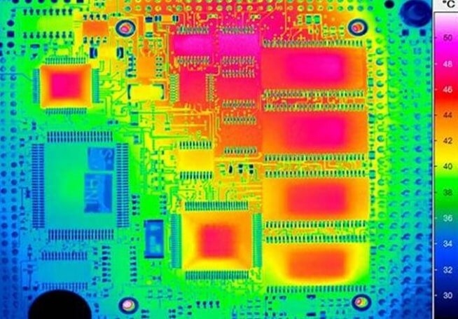
Thermal stress refers to internal stress generated by uneven thermal expansion or contraction when a material undergoes temperature changes. Thermal stress occurs when different parts of an object undergo uneven dimensional changes during heating or cooling, and these parts restrict each other's ability to deform freely. This stress is particularly pronounced in multilayer structures, systems with dissimilar materials, or systems subject to localized heating.
Thermal stress exists not only in high-tech fields such as large industrial equipment, bridge structures, and spacecraft, but is also prevalent in everyday electronic products, particularly printed circuit boards (PCBs), where thermal stress has a significant impact.

thermal stress
The Mechanism of Thermal Stress Formation
The generation of thermal stress can be explained by a mismatch in the coefficient of thermal expansion (CTE). A material's CTE determines its dimensional change per unit temperature change. If two materials (such as copper and fiberglass) are combined and heated simultaneously, they expand or contract at different rates. However, due to their bonded connection, they cannot deform freely, ultimately generating stress. In addition, the rate of temperature change (the speed of heating or cooling) also affects the magnitude of thermal stress. Rapid temperature changes can easily induce severe thermal stress, leading to material fatigue and even cracking.
Manifestations of Thermal Stress in PCBs
1. Board Warping/Bowing
One of the most visible manifestations of thermal stress is board warping during the heating or cooling process. For example, during the reflow soldering process, the PCB undergoes thermal cycles from room temperature to temperatures as high as 260°C. If the CTE of the materials between the layers is inconsistent, uneven thermal stress will occur, causing permanent deformation of the PCB. This can affect component placement accuracy and, in severe cases, lead to solder joint failure or fracture.
2. Plated Through Hole Cracking
Multilayer PCBs utilize numerous plated through holes (PTHs) to connect the circuit layers. The copper layers in the PTHs and the surrounding epoxy glass cloth substrate have different CTEs. During repeated thermal cycles (such as thermal shock tests or prolonged operation), thermal stress accumulates between the copper and substrate, eventually leading to microcracks or even through-hole fractures in the copper, impacting signal transmission reliability.
3. Pad Lifting
When PCB soldering temperatures are uneven or the pad is not firmly bonded to the substrate, thermal stress concentrates at the pad edges, easily causing the pad to separate from the board. Repeated heating during repairs can exacerbate this accumulation of thermal stress and lead to pad delamination.
4. Delamination
In multilayer PCBs, thermal stress can cause delamination between layers, resulting in voids (hollowing and delamination). This occurs because the thermal expansion coefficients of different materials, such as resin, copper foil, and fiberglass cloth, differ. Prolonged high-temperature operation or repeated thermal cycling can damage the interlayer structure.
5. Surface Cracks
For certain surface coatings, such as nickel-gold and tin, microcracks may develop after prolonged exposure to heat. These cracks can become the starting points for corrosion and electromigration, ultimately impacting electrical performance and reliability.
Thermal Stress in PCBAs
During the PCBA (Printed Circuit Board Assembly) process, thermal stress not only affects the bare board (PCB) itself but also significantly impacts component soldering quality, assembly reliability, and long-term stability. As electronic products evolve toward higher density, higher performance, and thinner designs, the impact of thermal stress becomes even more pronounced.
Typical Manifestations and Impacts of Thermal Stress in PCBAs
1. Solder Joint cracks or failures
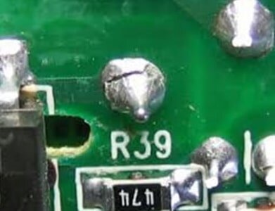
Excessive solder fatigue can lead to permanent cracks and fractures in solder joints, as shown in the figure. In the electronics industry, particularly in the defense sector, to ensure system reliability and as part of PCB thermal management in late development stages, electronics manufacturers purchase specialized temperature chambers to perform thermal cycling tests on PCB assemblies. PCBs that fail to consider the effects of thermal cycling during the design phase often fail after thermal cycling. Solder joint fracture is the most common cause of PCBA failure.
Modern electronic assemblies are often exposed to severe temperature conditions, such as the power supply for airborne radars. Repeated thermal cycling causes these electronic assemblies (including the PCB substrate, components, and solder joints) to undergo thermal contraction and expansion. Rapid contraction and expansion can cause thermomechanical fatigue, leading to solder deformation and subsequent solder joint degradation. Thermomechanical fatigue is a major cause of PCBA failure.

Solder cracks
2. Component Failure
BGA (Ball Grid Array) Solder Ball Fracture: Due to the different thermal expansion coefficients between the PCB and the chip package, the solder balls can fracture due to shear stress after repeated thermal cycles.
QFN/LGA Chip Solder Joint Debonding: Large-area packages with bottom soldering are prone to overall warping or edge failure due to thermal expansion and contraction.
3. Pad or Trace Debonding
Especially during rework, improper temperature control can cause pads to separate from the PCB substrate, seriously affecting solderability and reliability.
4. Board Warping, Leading to Misaligned Mounting or Cold Solder Joints
Board warping during heating can cause component misalignment, leading to poor soldering or short circuits in severe cases. 5. Internal device cracking or package cracking
Components such as ceramics, electrolytic capacitors, and inductors may crack under thermal stress, leading to changes in electrical performance or insulation failure.

thermal stress
As a key factor affecting the performance and reliability of PCBs and PCBAs, thermal stress plays a vital role throughout the entire electronics manufacturing process. From material selection and structural design to soldering processes and quality inspection, engineers must systematically consider the sources and control methods of thermal stress. As electronic products move toward higher density, miniaturization, and higher reliability, thermal stress issues are becoming increasingly prominent, manifesting as solder joint cracks, component failure, and board warping. In the future, with the help of thermal simulation, intelligent manufacturing, and new material technologies, the industry will achieve more refined and systematic breakthroughs in thermal stress management, thereby improving product stability.