With the continuous expansion of global data center scale and the rapid growth of AI accelerated computing demand, optical modules are playing an unprecedented important role as high-speed interconnection bridges between servers and switches. From 25G and 100G to 400G and 800G optical modules, their high-speed electrical interfaces require higher signal integrity, reliability, and processing technology for PCB.
In the highly integrated system of optical modules, PCB is not only the carrier of circuits, but also the key infrastructure that determines high-speed link performance and module stability.
The Core Role of PCB in Optical Modules
High-speed differential signal transmission: Connecting core ICs such as DSP, CDR, TIA, and laser driver.
Power isolation and noise suppression: Stabilizing and isolating multiple power supplies from interference.
Thermal management and heat dissipation path construction: Ensuring long-term operation of the module under high-power environments.
Mechanical and structural support for the photoelectric conversion area: Maintaining device positioning accuracy and overall module reliability.
With the rapid increase in optical module speeds, the material properties, layer stack-up structure, and processing capabilities of the PCB have become key factors affecting link performance.
Commonly Used PCB Materialsand Layer Stack-up Designs for High-Speed Optical Modules
To meet the requirements of high-speed signals such as 56G/112G PAM4, the industry has gradually transitioned from traditional FR4 to low-loss materials:
| Module Rate | Recommended Material | Dielectric Constant Dk | Loss Tangent Df | Features |
|---|---|---|---|---|
| 25G | High Tg FR4 | 4.2 | 0.01 | Low cost, suitable for mid-speed links |
| 56G | S1000H / MEGTRON 6 | 3.4 | 0.003 | Low loss, industry mainstream |
| 112G | Tachyon 100G / I-Speed | 3.2 | 0.002 | Ultra-low loss, high manufacturing requirements |
The typical characteristics of a stacked structure include:
The high-speed layer adopts ultra-thin dielectric (reducing wiring loss)
Laser blind holes and buried holes meet high-density interconnection requirements
Backdrill reduces reflection caused by residual stubs in via holes
Multi layer design for EMI suppression
These designs collectively ensure that the insertion loss and return loss of high-speed links meet the requirements of the IEEE 802.3 series standards.
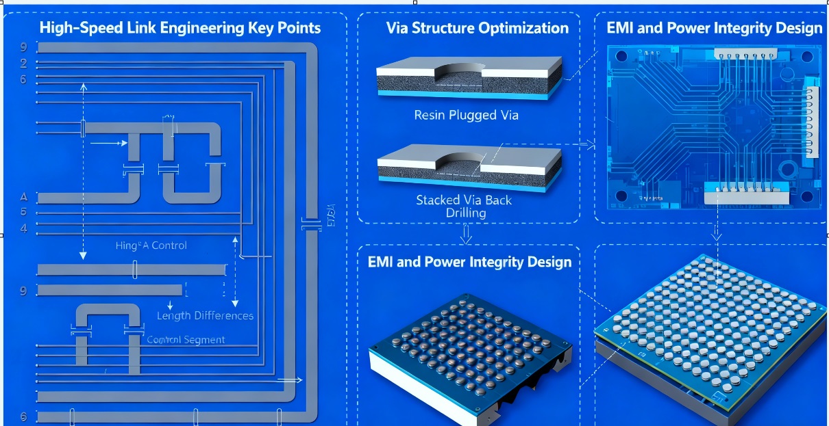
Optimization of via structure
Differential routing design
Accurate impedance control (typically 85 Ω± 5%)
Control the length difference at the sub mil level
Using circular arcs or a 45 ° angle to avoid excessive radiation caused by a 90 ° angle
Optimization of via structure
High speed signals are extremely sensitive to vias, so the industry generally adopts:
Type VII resin filled via
Stacked via for high-density packaging
Backdrill eliminates through-hole stubs to improve reflection performance

Key points of high-speed link engineering design
EMI and power integrity
Power partition isolation
Local shielding cover is used in high-frequency areas
Surrounding ground via array (GND stitching)
Special requirements of PCB for different optical module structures
The packaging forms of optical modules are diverse, and the internal structural differences directly affect the PCB design method.
COB (Chip On Board) solution
Key features:
DSP/TIA bare chip directly soldered onto PCB
The requirement for solder mask accuracy is extremely high
The gold wire has a short span and strict requirements for geological layout
ACO (Active Cooled Optics) solution
Suitable for scenarios with extremely high temperature control requirements:
Add TEC and NTC related layouts
Strengthen the design of metal heat dissipation paths
PCB needs to ensure stability under thermal stress
TO-CAN packaging solution
Key Features:
Strict requirements for coaxial shielding structure
High frequency devices need to be arranged nearby
Grounding design must maintain extremely low impedance
Thermal Design and Structural Reliability
The overall size of the optical module is small and the power density is high, making the thermal management capability of the PCB crucial.
Thermal design measures include:
Thermal conductivity between large-area copper foil and copper-clad islands
Design of Via in Pad with Multiple Via Arrays
Increase the coupling efficiency of thermal interface materials (TIM)
Reliability enhancement measures:
Select substrates with excellent CAF performance
Moisture resistant design (solder mask material, edge sealing)
Golden Finger adopts ENIG/ENEPIG technology to improve the insertion and removal life
The future development direction of optical module PCB
Driven by the demand for high-speed interconnection between AI data centers and the next generation, optical module PCBs are evolving in the following directions:
Lower loss materials: LCP, mSAP, ABF substrates will gradually become popular
Higher Density Interconnection (HDI/SLP): Suitable for module heights below 1.0 mm
Optoelectronic Hybrid Integration (CPO): Deep Collaboration between PCB and Light Engine
Higher automation production and quality control: supporting consistency at the million wafer level