A solder stencil is a stencil used in the SMT (surface mount technology) process. Its primary function is to accurately print solder paste on PCBs (printed circuit boards), ensuring that the paste is applied only to component pads.
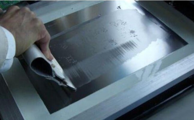
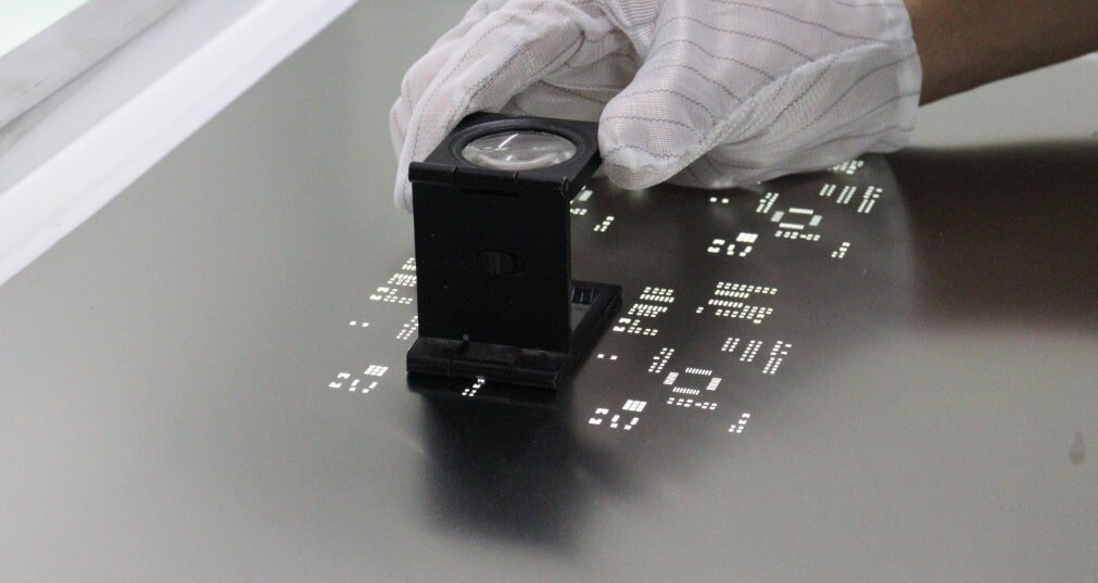
A solder stencil is a metal template used to precisely print solder paste on PCBs during SMT. Typically constructed from tin-bronze or stainless steel, its thickness and apertures are precisely designed based on the PCB pad size and solder paste volume requirements. The manufacturing process involves laser etching or chemical etching to ensure that the aperture position, shape, and size exactly match the design. During soldering, the stencil is placed over the PCB surface, and solder paste is evenly applied using a jet printer, forming solder bumps that are then used for component placement and reflow soldering. Currently, most popular circuit boards, with the exception of power supply boards, utilize surface mount technology (SMT). These PCBs feature numerous label pads (i.e., no vias). The holes in the stencil correspond precisely to the component pads on the PCB. Manual solder paste printing involves horizontally applying a semi-liquid, semi-solid solder paste through the holes in the stencil onto the PCB. Components are then mounted using a placement machine, followed by reflow soldering. The final product is what's known as a PCBA (Printed Circuit Board Assembly) circuit board!

solder stencil
Common Types:Laser Stencils: Produced using laser cutting technology, they offer high precision and are suitable for complex printed circuit boards.
Chemically Etched Stencils: Produced using chemical etching technology, they are relatively low-cost and suitable for simple printed circuit boards.
Electroformed Stencils: Produced using electroforming technology, they offer excellent durability and precision and are suitable for demanding printed circuit boards.
The following factors affect the quality of PCB stencils:
1. Manufacturing Process. Previously, we discussed the stencil manufacturing process. We know that the best process is to electropolish the stencil after laser cutting. Both chemical etching and electroforming involve processes such as film preparation, exposure, and development that are prone to errors. Electroforming is also affected by substrate unevenness.
2. Materials Used: These include the PCB stencil frame, screen, steel sheet, and adhesive. The PCB stencil frame must be able to withstand a certain amount of tension and maintain good levelness. Polyester screen mesh is preferred, as it maintains stable tension over time. 304 steel sheet is preferred, and a matte finish is more conducive to solder paste (adhesive) rollability than a mirror finish. The adhesive must be strong and resistant to corrosion.

stencil
3. Aperture Design: The quality of the aperture design has the greatest impact on the quality of the PCB stencil. As discussed earlier, aperture design should consider the manufacturing process, aspect ratio, area ratio, and empirical data.
4. Production Data: The completeness of the production data also affects the quality of the PCB stencil. The more complete the data, the better. Furthermore, when multiple data sources exist, it should be clearly defined which one should be used. Furthermore, generally speaking, creating the stencil from a data file minimizes errors. 5. Usage: Proper printing methods maintain stencil quality. Conversely, improper printing methods, such as excessive pressure or uneven PCB stencil or PCB during printing, can damage the stencil.
6. Cleaning: Solder paste (adhesive) solidifies quickly. If not cleaned promptly, it can clog the stencil openings, making the next printing process difficult. Therefore, the PCB stencil should be cleaned immediately after being removed from the machine or after an hour without solder paste printing on the printer.
7. Storage: Stencils should be stored in designated areas and not randomly placed to prevent accidental damage. Also, PCB stencils should not be stacked on top of each other, as this makes handling difficult and may cause bending of the stencil frame.
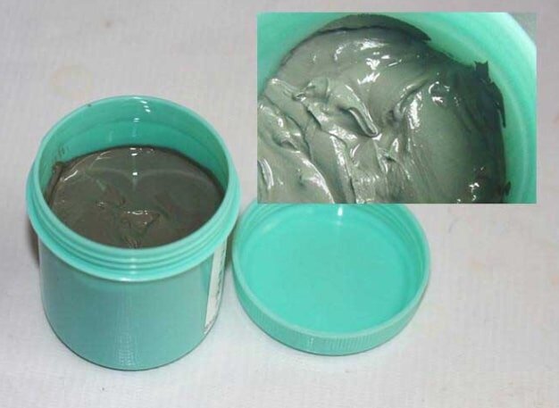
Solder paste looks like this:

solder
Before placement, solder paste is printed onto the PCB pad surface using an SMT laser stencil (the stencil is a fixed quantity, and batch printing improves efficiency).
Solder stencil plays a crucial role in the SMT production process. First, the cleaned and surface-treated PCB is placed under the stencil to prepare it for solder paste printing. Subsequently, solder paste is evenly applied to the stencil's openings using a specialized scraper, depositing it precisely onto the PCB's pads to ensure subsequent placement accuracy. Next, a placement machine, according to program settings, accurately places various electronic components onto the solder paste, forming the initial assembly structure. The PCB then enters the reflow oven, where the solder paste melts at high temperatures, forming a secure electrical and mechanical connection. Finally, the PCBA undergoes a comprehensive inspection using automated optical inspection (AOI), X-ray inspection, and functional testing to ensure product quality and reliability. This entire process is efficient and precise, and is the core of modern electronics manufacturing.
As an indispensable link in the SMT production chain, solder stencil, with precision, efficiency, repeatability, and flexible customization, are crucial tools for improving PCBA quality and reducing costs.