What is a stencil?
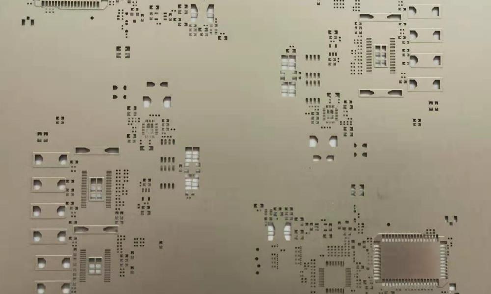
The most important function of a stencil is to assist in the deposition of solder paste, transferring the exact amount of solder paste or red glue to the exact location on an empty PCB.
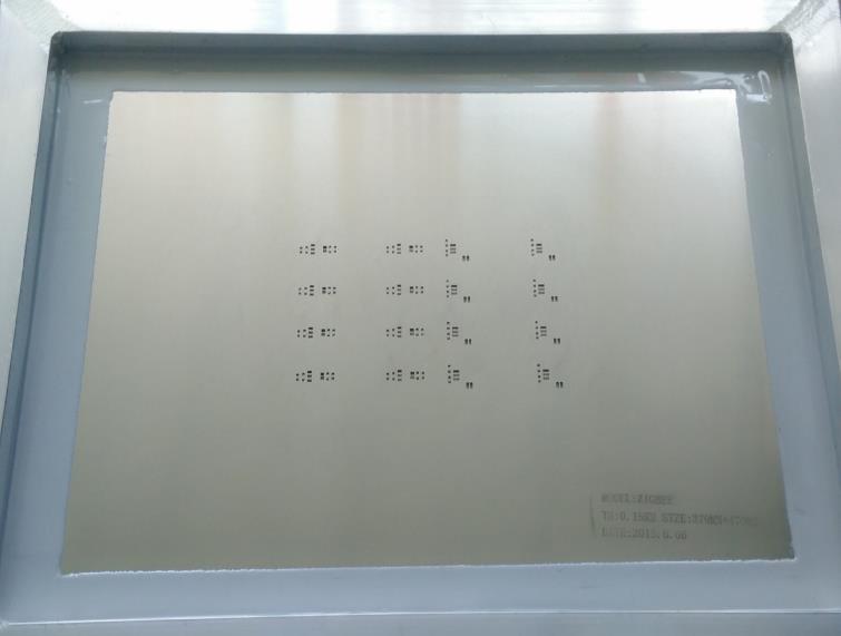
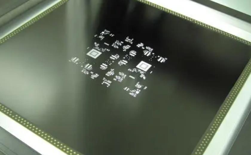
A stencil is a printing method to facilitate the printing of solder paste onto a PCB, somewhat similar to the principle of a rubber stamp or seal. Stencils are designed with certain rules before they are formed and laser cut into stencils. Therefore, a stencil is an auxiliary tool. A stencil is a very thin piece of steel, the size of the stencil is generally fixed to match the solder paste printing machine, but the thickness of the stencil ranges from 0.08mm, 0.10mm, 0.12mm, 0.15mm, 0.18mm and so on.

SMT stencil
The use of the stencil
We often say PCBA, is in the PCB will be specific electrical performance components, in accordance with the setting of the BOM,bit number and other information; according to the rules of the paste, and then through the solder paste will be components at each end of the welding, or the use of red glue on the positioning of components, through the wave soldering welding through the formation of the circuit board set to achieve the initial circuit function, so that the product has a certain level of performance and to improve productivity. The main purpose of the stencil is to make the product have a certain performance and improve productivity.
The main purpose of the stencil is to allow solder paste to be printed on the circuit board and designed, the top side of the stencil will be engraved with a lot of holes, when printing solder paste, you have to rub the solder paste on the top of the stencil, and the circuit board will be placed on the bottom side of the stencil, then use a scraper (usually a scraper, because the solder paste is similar to toothpaste-like thick material) to brush over the top side of the stencil with solder paste, the solder paste suffers from the squeeze and will flow downward and stick to the holes of the stencil. When the stencil is squeezed, the paste will flow down through the holes of the stencil and stick to the top of the board. When the stencil is removed, you will see that the paste has been printed on the board. To put it simply, the stencil is like a cover that you have to prepare in advance when spraying paint, and the solder paste is equivalent to the paint, with the pattern you need engraved on the cover, and the pattern will be displayed when you spray the paint on the cover.
Sourcing a stencil is not only a step in the assembly process, it is also an important step. The main function of the stencil is to help with the deposition of the solder paste. The purpose is to transfer the exact amount of data to the exact location on the bare PCB. The less solder paste is blocked on the stencil, the more it is deposited on the board. Therefore, when something goes wrong during the printing process, the reaction is to blame the stencil. However, it should be remembered that there are more important parameters than the screen that can affect its performance. These variables include the printing machine, the particle size and viscosity of the solder paste, the type, material, hardness, speed and pressure of the squeegee, the separation of the stencil from the PCB (sealing effect), the flatness of the soldermask, and the flatness of the component.
Stencil Manufacturing Technology
The three main technologies used in pcb stencil manufacturing are chemical etching (etch), laser cutting, and electroforming. Each has unique advantages and disadvantages.Chemical etching and laser cutting are substractive processes, electroforming is an incremental process.Therefore,comparisons of certain parameters, such as price, may be an apples-to-oranges comparison.However,the main consideration should be performance in relation to cost and cycle time.
Generally, chem-etched stencils and other technologies are equally effective when used in applications with tight spacing of 0.025’ or more.Conversely,laser cut and electroforming screens should be considered when dealing with pitches below 0.020’. While the latter types of stencils work well for pitches above 0.025’, the price and cycle time may be difficult to justify.
Chemically etched screens
Chemically etched stencils are the main type of stencil in the world of stencils.They are cost effective and have a fast turnaround time.A chemically etched stainless steel screen is produced by applying a corrosion inhibitor to the metal foil, exposing the image to both sides of the foil with a pin-positioned photographic tool, and then etching the foil from both sides simultaneously using a double-sided process. Because the process is double-sided, the etchant penetrates through the holes, or openings, created in the metal.
As the process is two-sided, the etchant penetrates through the holes,or openings,created in the metal and etches not only from the top and bottom sides, but also horizontally. Inherent in the technology is the formation of a blade, or hourglass shape (Figure 1). This shape creates an opportunity to block the solder paste when spaced below 0.020’,a defect that can be minimised by an enhancement process called electropolishing.
Electropolishing is an electrolytic back-end process that ‘polishes’ the walls of the holes, resulting in reduced surface friction, good paste release and fewer voids. It also greatly reduces cleaning of the underside of the stencil. Electropolishing is achieved by attaching the metal foil to an electrode and immersing it in an acid bath.The current causes the etchant to first etch the rougher surfaces of the holes, which has a greater effect on the walls of the holes than on the top and bottom surfaces of the foil, resulting in a ‘polished’ effect (Fig. 2).The metal foil is then removed before the etchant acts on the top and bottom surfaces. In this way, the surface of the hole wall is polished and the antique film is effectively rolled (not pushed) across the surface of the stencil by the squeegee and fills the hole.
Another technology for improved solder paste release for pitches up to 0.020’ is trapezoidal section apertures (TSA).
Trapezoidal section apertures (TSA) are openings in the stencil where the contact (or bottom) side is 0.001 to 0.002’ larger than the squeegee (or top) side (Fig. 3).Trapezoidal cut-off holes can be accomplished in one of two ways: by selective trimming of special components, i.e.,the contact side of the double-sided developing tool is made larger than the squeegee side;or by stenciling all trapezoidal cut-off holes,which can be produced by varying the pressure settings on the top and bottom sides of the etchant spray.When electropolished,the geometry of the hole walls allows solder paste to be released at intervals of 0.020’ or less.Additionally,the resulting solder paste deposit is a trapezoidal ‘brick’ shape, which promotes stable component placement and less solder bridging.
Stepdown,or dual-level,stencils can be easily produced by chemical etching technology.The process reduces the amount of tin in a selected component by forming a step-down hole.For example,in the same design,a few 0.050‘~0.025’ pitch components (typically requiring a 0.007‘ thickness stencil) are grouped together with a few 0.020’ pitch QFPs (quad flat packs). In order to reduce the amount of solder paste on the QFPs,this 0.007‘ thickness stencil creates a 0.005’ thickness downstage area. The downstage should always be on the squeegee side of the stencil, as the contact surface of the stencil must be horizontal across the board (Figure IV). Nevertheless, it is recommended to provide at least 0.100’ separation between the QFP and the surrounding components to allow the squeegee to fully dispense solder paste on both levels of the stencil.
Chemically etched screens are also useful for producing half-etched fiducials and caption names.Datums for printer visual system alignment can be half-etched and then filled with black resin to provide a contrast with the smooth metal background that is easily recognised by the visual system.Caption blocks containing the part number,date of manufacture and other pertinent information can also be half-etched onto the stencil for labelling purposes.Both processes are accomplished by developing only half of both sides.
Limitations of chemical etching.In addition to the drawbacks of blade-shaped edges, chemically etched screens have another limitation: the aspect ratio. Simply put,this ratio limits the number of hole openings that can be etched according to the thickness of the metal at hand.Typically,for a chemically etched stencil, the aspect ratio is defined as 1.5:1.Thus,for a stencil with a thickness of 0.006‘, the hole opening would be 0.009’ (0.006‘ x 1.5 = 0.009’). In contrast, for electroformed and laser cut stencils,the aspect ratio is 1:1, i.e., a 0.006‘ opening can be produced on a 0.006’ thickness stencil by either process.

stencil
Electroforming
Electroforming, an incremental rather than decremental process, produces a nickel-metal stencil with unique gasketing characteristics that reduce solder bridging and the need for stencil underside cleaning. The process provides near-perfect positioning without geometric constraints, has inherently trapezoidal smooth aperture walls and low surface tension for improved solder paste release.
This is achieved by developing photoresist on a substrate (or mandrel) on which the apertures are to be formed, and then electroplating the stencil around the photoresist atom by atom, layer by layer. As seen in Figure 5, the nickel atoms are deflected by the photoresist, creating a trapezoidal structure. Then, when the stencil is removed from the substrate,the top surface becomes a contact surface, creating a sealing effect. A continuous nickel thickness in the range of 0.001 ~ 0.012’ can be selected. The process is ideal for ultra-fine-pitch requirements (0.008 ~ 0.016") or other applications. It achieves an aspect ratio of 1:1.
As for the defects, since it involves a photographic tool (albeit single-sided) there may be malposition. If the plating process is not uniform, the sealing effect will be lost. Also, the sealing ‘block’ may be removed if the cleaning process is too aggressive.
Laser cut stencils
Generated directly from the customer's original Gerber data, laser-cut stainless steel stencils are characterised by the fact that there is no photographic step. This eliminates the chance of misalignment. Stencils are produced with good positional accuracy and reproducibility. The Gerber file, with the necessary modifications, is transferred to (and directly driven by) the laser machine. Less physical interference means less chance of error. Although the laser beam produces
Although there is a major problem with metal slag (evaporated molten metal) produced by the laser beam, today's laser cutters produce very little slag that can be easily removed.
There is also the problem of a ‘scalloped’ shape around the hole, resulting in a rough hole wall. Although this increases surface friction, the roughness is in the vertical plane.However, recent laser machines have an internal vision system that allows the foil to be cut without a border.This makes sense because the stencil can be made by chemically etching standard-pitch components and then laser cutting fine-pitch components. This ‘hybrid’ or combined stencil offers the advantages of both technologies, lower cost and faster turnaround.In addition, the entire stencil can be electropolished to provide smooth hole walls and good solder paste release. The main disadvantage of the laser cutting process is that the machine cuts each hole individually. Naturally, the more holes there are, the longer it takes and the higher the cost of the stencil. Nevertheless, if the design permits, costs can be reduced by utilising a hybrid stencil process. Trapezoidal holes are automatically created by following the focus of the laser beam.The hole openings are actually cut from the contact side of the stencil; the stencil is then turned over and mounted squeegee side up.
Laser technology is a process that allows existing screens to be reworked,such as enhancing holes,enlarging existing holes or enhancing datums.
Other Advances in Stencils
In addition to laser cutting and electroforming, an important advancement in screen production is electronic data transfer. As recently as 1995, most of the images supplied to screen manufacturers were film positives, which matched the image on the photocopier one-to-one. The retouching of component apertures involves a great deal of photographic skill and handwork. The process is also determined by the quality of the film positive supplied. The step-by-step reproduction of the image is a tedious task.
Today, electronic file transfer via modem and e-mail is a common method of providing graphic data in real time. Selective retouching, step-by-step graphic repetition, and geometric shape conversion can be easily and readily accomplished. And, by eliminating the mailing of film positives, turnaround time can be cut by almost a full day.
With the Gerber file transfer, the geometry of pads can be changed from squares and rectangles to ‘home plate’, ‘grid’, ‘zip’, etc. (Figure 1) The geometry of the pad can be changed from square and rectangle to ‘home plate’, ‘grid’, ‘zip’, etc. (Fig. 6) as a way to reduce the amount of solder paste. Adjusting the amount of solder paste by modifying the geometry, combined with selecting the correct thickness of the metal plate, also eliminates the need for a stepdown plate. Single Thickness Stencils
A single thickness stencil, properly designed, is always better from a process point of view than a two-stage tool.
Adhesive Stencil
Electronic files also make it easy for the computer-aided design (CAD) operator to determine the centre of mass of a pad shape. With this capability, the solder paste layer in the design file can be converted to round and elliptical shapes. The design file can be used to determine the size of the component (Fig. 7). Instead of glue drops, a stencil can be made to ‘print’. Printing is faster than gluing, leaving this equipment for other work.
Rework Web Edition
A relatively recent innovation has occurred in the area of rework. There are now ‘mini’ stencils designed specifically for rework or refurbishment of individual components. Stencils can be purchased for individual components such as standard QFPs and ball grid arrays (BGAs). Of course, there are also corresponding squeegees, or small squeegees.

stencil
Stencil Price Comparison
The price of a chemical etching stencil is driven by the size of the frame. While the foil is the focal point of the screen production process, the frame is a single, expensive fixed cost. The size is largely determined by the type of press. However, most printers can accept more than one frame size. (Frame sizes are an industry standard). Most stencil suppliers maintain an inventory of standard frames ranging in size from 5x5‘ to 29x29’. Because the cost of empty foil is not as great as the cost of frames, the thickness of the metal has no effect on the price. And since all the holes are etched at the same time, the number of holes is irrelevant.
The price of an electroformed stencil is primarily driven by the thickness of the metal. Plating to the desired thickness is the main consideration: thicker stencils cost less than thinner ones.
The price of laser cut stencils is based on the number of holes designed.
The more holes a laser cuts, i.e. the more holes, the higher the cost. Also add the required frame size.A hybrid stencil with laser cut close spaced and chemical corrosion standard spaced components may be a cost effective method when many holes are required. However, for designs with less than 2,500 holes, it may be more cost effective to laser cut the entire stencil.
In summary, whatever the needs of the PCBA process may be,there is currently a stencil technology that meets that need.Some of the innovations discussed, such as trapezoidal perforations, hybrid stencils, and the advantages of electronic data transfer, have been developed and improved over the last three or four years.The stencil industry has traditionally been not only responsive to new requirements, but also ahead of the curve in these ongoing developments.