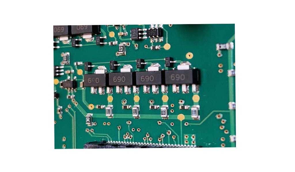
PCB reverse engineering, also known as circuit board copying, circuit board cloning, circuit board replication, PCB cloning or PCB reverse research and development, is a technical process of reverse analysis of circuit boards using reverse research and development technology on the premise of existing electronic products and circuit boards. This process aims to restore the original product's PCB files, bill of materials (BOM) files, schematic files and other technical files and PCB silk screen production files to achieve 1:1 replication. Subsequently, these technical files and production files are used for PCB board making, component welding, flying probe testing, and circuit board debugging, and finally complete the complete replication of the original circuit board sample.
Specifically, the process of PCB reverse engineering includes the following key steps:
1. Sample acquisition and scanning: First, it is necessary to obtain the physical object of the target electronic product or the physical object of the circuit board. Then, use high-precision scanning equipment to scan the circuit board to obtain its detailed physical structure and circuit layout information.
2. Data extraction and analysis: Extract and analyze the scanned data through professional reverse engineering software. This process includes identifying all components on the circuit board, analyzing the circuit layout, simulating circuit functions, etc.
3. Technical file restoration: Based on the data obtained from the analysis, the reverse engineer will restore the original PCB file, schematic file, BOM file and other key technical files. These files are the basis for the subsequent replication of the circuit board.
4. Production and debugging: Use the restored technical files and production files to carry out the production process such as PCB board making and component welding. Subsequently, through steps such as flying probe testing and circuit board debugging, ensure that the copied circuit board is consistent with the original circuit board in terms of function and performance.

PCB reverse engineering plays an important role in the following aspects:
1. Technology learning and R&D acceleration: Through reverse engineering, companies can quickly obtain and analyze the product technical details of competitors or industry leaders. This helps companies understand the cutting-edge technology in the market, accelerate the R&D process of their own products, and shorten the product launch cycle. At the same time, reverse engineering can also help companies discover technical bottlenecks and potential innovations, and provide direction for subsequent technical research and development.
2. Fault analysis and repair: When an existing product fails or is damaged, PCB reverse engineering can analyze the structure and circuit layout of the circuit board in detail and quickly locate the fault point. This helps companies repair products quickly and reduce losses caused by failures. In addition, reverse engineering can also help companies understand the design defects and potential problems of products, providing a basis for subsequent improvements and optimizations.
3. Compatibility and upgrades: In some cases, companies may need to make old products compatible with new systems or equipment. Through PCB reverse engineering, companies can understand the circuit design and interface specifications of old products, so as to design new products or upgrade solutions that are compatible with them. This helps companies maintain the market competitiveness of products and extend the life cycle of products.
4. Cost control and supply chain management: Reverse engineering can help companies understand the bill of materials (BOM) and component information of products, thereby optimizing supply chain management and reducing procurement costs. By understanding the design details and manufacturing processes of products, companies can also optimize the production process, improve production efficiency, and further reduce costs.
PCB reverse engineering is of great significance in the repair, imitation and improvement of electronic products, especially in the absence of original design documents. However, it should be noted that PCB reverse engineering must be carried out under the premise of respecting intellectual property rights. When using reverse engineering technology, companies should abide by relevant laws, regulations and ethical standards to ensure that they do not infringe on the legitimate rights and interests of others. Furthermore, reverse engineering should be used primarily for positive purposes such as technology learning and R&D acceleration, rather than for illegally copying or selling other people's products.