A Trustworthy PCB and Electronic Manufacturing Enterprise! Contact Us


1. Transistor packaging basics
Transistor manufacturing involves wafer fabrication, wafer testing (probe/sorting), wafer packaging (assembly), testing, and finally, warehousing of finished goods.

Transistor manufacturing process flow
1.3. Encapsulated functions
The most basic function of packaging is to protect the circuit chip from the effects of the surrounding environment (including physical and chemical effects). Therefore, in the initial microelectronic packaging, Metal Can was used as the shell to protect fragile electronic components in an air-tight manner that was completely isolated from the outside world. However, with the development of integrated circuit manufacturing processes, especially the continuous improvement of the wafer passivation layer manufacturing process, the functions of packaging are slowly becoming alienated.

Three levels of microelectronic packaging
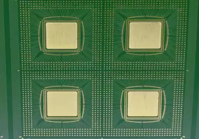
Electronic packaging involves complex systems with diverse materials and processes, categorized by geometric dimensions like "point, line, surface, body, block, and board". Electronic substrates serve as the foundation for transistor chip packaging, supporting electronic components such as PCBs and module substrates. The rise of laminated multilayer boards has expanded substrate options. Package substrates (PKG substrates) like BGA, CSP, TAB, and MCM are newer module substrates mounted on PCBs, supporting various packaging formats. These substrates not only support chips and components but also underpin entire electronic circuit systems, necessitating advancements in high-density multilayer substrates for improved functionality and performance in electronic packaging engineering.

Transistor packaging process
The essence of chip packaging technology is to provide a stable protective environment for integrated circuit chips while establishing an effective connection with external circuits. The packaging process includes steps such as chip slicing, pin connection, and packaging shell formation. It is designed to protect the chip from the impact of the external environment and achieve low-noise and low-latency signal transmission between circuits. With the advancement of technology, packaging technology is continuously optimized, chip size is reduced, pin density is increased, and temperature resistance and reliability are improved.

Commonly used packages
The development history of transistor packaging technology can be divided into three stages:
1. The first stage (before the 1970s): mainly through-hole plug-in packages, such as metal round (TO type) and ceramic dual in-line package (CDIP), among which plastic dual in-line package (PDIP) became the mainstream product.
2. The second stage (after the 1980s): the introduction of surface mount packages, such as plastic lead chip cut-out (PLCC) and plastic quad flat package (PQFP), promoted the development of packaging forms towards higher density and efficiency.
3. The third stage (after the 1990s): the size of transistors reached ultra-large-scale integration, and the lead pipeline changed from planar quad lead type to planar ball grid array package (BGA), which promoted the emergence of new packaging technologies such as chip level packaging (CSP) to meet the needs of miniaturization and high performance.
In general, transistor packaging technology has continued to evolve with the development of electronic devices, from traditional plug-in packaging to modern surface mount and ball grid array packaging, continuously improving packaging density, efficiency and functionality.
, plastic packaging (P)")
Metal packaging, ceramic packaging (C), plastic packaging (P)
In microelectronic packaging, chip electrical interconnection is a key link to ensure device reliability. The main interconnection methods include wire bonding, tape automated bonding, and flip-chip bonding. Although TAB and FC have good electrical performance, they are mainly used for chips with few I/Os or specific requirements due to the high cost of equipment. In contrast, WB occupies a mainstream position in chip electrical interconnection, especially for stacking interconnection of chips in 3D packaging.
 interconnect")
Chip electrical (zero-level packaging) interconnect
Pin Thread Thread (PTH) packaging is a traditional form of packaging that uses vias to connect the die to the target board. Classic DIP packaging belongs to this type of packaging. Early integrated circuits usually chose this packaging form due to their small number of pins. Derivatives of DIP packages include SIP and ZIP, which have improvements in pin arrangement and shape to adapt to different application fields.

DIP,SIP,ZIP package
3.2 Surface Mount Technology (SMT)
Is a modern packaging technology that occupies less effective wiring area in PCB design than traditional PTH packaging. Common surface mount packages include small plastic transistor (SOT), small outline package (SOP), quad flat no-lead package (QFN), thin small shrink outline package (TSSOP), quad flat package (QFP) and quad flat no-lead package. Pin package (QFN), etc. The number of pins and pin spacing supported by these packaging forms are gradually increasing, resulting in a reduction in chip package size and an increase in pin density. The main advantages of surface mount packaging are small size and high pin density. It is suitable for multi-layer wiring processes and can significantly improve the wiring density and utilization of PCB boards.

SMT Package
BGA package uses ball pins arranged at the bottom of the package, which meets the needs of high-density and small-size chips. It has the advantages of low failure rate, small package size, excellent pin coplanarity, avoiding pin deformation, reducing resistance/capacitance/inductance effects, improving heat dissipation and high packaging density. It is one of the mainstream packaging forms of modern large-scale integrated circuits.

BGA Package
3. CSP (wafer level packaging) technology achieves high performance and high reliability requirements by packaging the chip in a package that is extremely small and close to the size of a bare chip, while minimizing the size of the package. It supports the configuration of more than 2,000 pins and has excellent thermal conductivity and optimization of signal conduction distance, adapting to the needs of modern high-frequency memory chips.

CSP packaging structure
4. Stacked packaging technology uses mechanical and electrical assembly methods to exponentially increase memory capacity or realize multi-functional electronic designs in a limited space, solving the problem of limited space and interconnection. It is divided into two types: custom stacking and standard commercial stacking. The former is more expensive but can achieve high-density layer processes, while the latter is slightly lower cost and is usually used for chip stacking packaging to improve memory module performance.

Multi-chip packaging structure
4.1 Stacked packaging technology mainly uses the stacking of wafers to achieve high integration and save space. Among them, PoP stacking (Package on Package) uses fully tested and packaged wafers, which has the advantage of high yield and each device can be tested individually before assembly; while PiP stacking (Package in Package Stacking) uses module stacks for simple testing and is low cost. lower. 3D packaging technology further improves the density and efficiency of packaging, enabling multi-chip stacking or multi-layer packaging in a smaller and thinner packaging volume.
4.2 Wafer-level packaging (WLP) is a technology in which most operations during the packaging process are performed on the wafer. There are two main types: fan-in and fan-out.
4.3 Fan-in WLP is packaged when the wafer is not cut. The size of the device is the same as the die size of the wafer, which is suitable for applications with low I/O count and smaller size.
4.4 Fan-out WLP is divided into two processes: wafer first and wafer last. The chip is placed first and then the wiring is carried out, which is usually used to improve the utilization rate of the chip; while the chip is placed later, the wiring is carried out first and then the chip is placed, which is more complicated but helps to improve the yield rate.
These technologies are designed to achieve smaller package sizes, reduce costs, and improve performance. They are one of the key technologies for today's highly integrated electronic products.

Two types of WLP processes
SiP (System in Package) and SoP (System on Package) are packaging technologies that have developed rapidly in recent years, especially suitable for consumer electronics and mobile communication products. Characterized by high density, low power consumption, miniaturization, heterogeneous integration and low cost, they have become an important process solution for achieving high-performance system integration. SiP/SoP packaging has a wide range of application markets and development prospects in the field of microelectronics, and is one of the main process solutions that will surpass Moore's Law in the future.

SIP encapsulation classification
Multi-chip component packaging (MCM) is a key technology for system-level packaging. Two or more chips are interconnected through a substrate to form a complete functional package. This technology effectively solves the challenges brought by the increasing functional complexity of the chip and can support product miniaturization and high performance requirements.
The above is what we have shared about the industry status and development of transistor packaging substrates. For more information on transistor packaging substrates, please click: IC package subatrates.