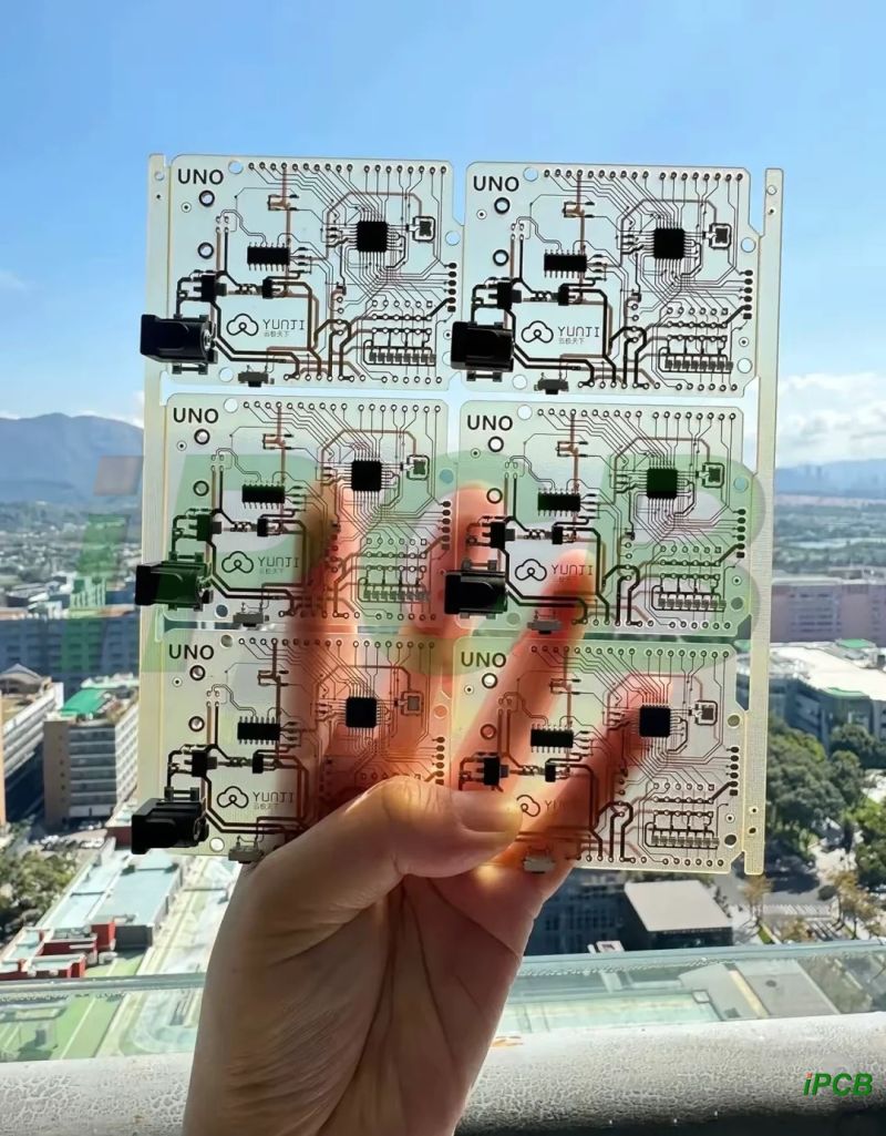
Transparent pcb board made of transparent substrate (such as glass, polyimide or plastic) and transparent conductive material (such as ITO, silver nanowire), which has both conductivity and light transmittance and is widely used in flexible display, smart touch and medical equipment. Transparent pcb is used to form electronic circuits and electrical connections. Transparent boards provide excellent optical fiber fields and do not experience light attenuation. They do not require heat sinks, can be made in large areas, have low dielectric losses, and are relatively easy to manufacture.
Transparent pcbs are made of a variety of materials. The most common material used to make these circuit boards is glass. Glass comes from a mixture of sand, ash, limestone and soda water.
Other materials can be used to make transparent circuit boards, such as sapphire glass or ceramic pcbs. :Sapphire glass is the strongest and hardest of all glass variants. Transparent ceramic circuit boards are made of a variety of materials. The most common materials used for this purpose include yttrium oxide, Aron, aluminum oxide or alumina, magnesium oxide, aluminum magnesium spinel, etc.
The following is a method for preparing a transparent pcb board, which is characterized by comprising the following steps:
(1) opening evenly distributed and penetrating conductive holes on a glass substrate;
(2) installing a hollow copper tube in the conductive hole that matches the size of the conductive hole and has a length equal to the thickness of the glass substrate, and making the end face of the hollow copper tube flush with the surface of the glass substrate;
(3) preparing a conductive paste with a mass ratio of 65-75:3:5-10:10-20:1-3 using conductor powder, low-temperature glass powder, ethyl cellulose, pine alcohol and dibutyl maleate, and printing the conductive paste on one of the planes of the glass substrate;

(4) baking the glass substrate with the conductive paste printed on one side at a temperature of 120-150°C for 100 ~300 seconds to solidify the conductive paste;
(5) Print the conductive paste on the other plane of the glass substrate, then bake the glass substrate with the conductive paste printed on both sides at a temperature of 120~150℃ for 100~300 seconds to solidify the conductive paste on both planes;
(6) Place the glass substrate in a temperature environment of 550~600℃ for 300~360 seconds, then place it in a temperature environment of 710~730℃ for 120~220 seconds, and finally cool it to room temperature to melt the conductive paste and the glass substrate into one to form a conductive circuit. The conductive circuit is distributed on the surface of the glass substrate and becomes a part of the glass substrate. The two conductive circuits are electrically connected through the hollow copper tube to obtain a transparent glass-based double-layer circuit board.
The present invention provides a method for preparing a transparent pcb board, which can realize the preparation of a transparent glass-based double-layer circuit board. The light transmittance of the prepared transparent glass-based double-layer circuit board exceeds 90%, has superconductivity, and the conductive impedance is less than 5×10⁻⁸Ω. The prepared transparent glass-based double-layer circuit board has no dielectric bonding, so that the circuit layer has good thermal conductivity when applied at high power, and the circuit layer is tightly fused with the glass plate molecules, and SMD electronic components can be mounted and the components are not easy to peel off.
Advantages of transparent glass pcbs compared with traditional pcbs
Transparent glass pcbs have several other advantages over traditional pcbs.
It is easy to see what is inside the circuit board because transparent pcb has better visibility than traditional opaque pcbs. They also allow you to easily identify components that may be hidden by opaque boards when installed in a housing or casing, such as resistors, capacitors and other components.
Transparent boards also allow you to easily identify jumper pins or other connections between layers of multilayer boards, making it easier to solve interlayer connection problems.
The application of transparent pcb boards is becoming more and more extensive. In recent years, we have actively developed and officially launched new transparent pcb boards, which have attracted widespread attention in the industry. Transparent pcb boards not only have significant advantages in performance, but their unique appearance design also adds infinite charm to the new generation of electronic devices.