The experiment examined the effects of high temperature and time on the device under long-term storage conditions of the wafer. This specification applies to the HAST test requirements during the mass production chip verification test phase, and is only applicable to tests of non-sealed packages (plastic packages), with bias (bHAST) and without bias (uHAST).
In the test, the reliability of non-sealed packaged devices in a high-temperature, high-pressure, and humid environment when powered on is evaluated through accelerated conditions of temperature, humidity, and atmospheric pressure. It adopts strict temperature, humidity, atmospheric pressure and voltage conditions, which will accelerate the electrochemical reaction between moisture penetrating into the material and the metal conductor.
HAST test standards
JESD22-A110E HAST test standard
JESD471 overall reliability standard
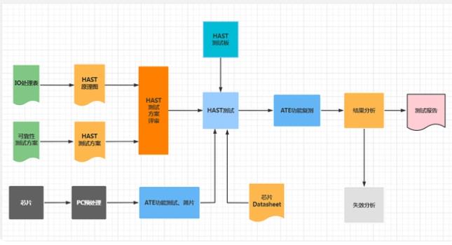
HAST testing process

HAST test conditions
1. The HAST test conditions of temperature, humidity, air pressure, and test time are as shown in the following table:

HAST high-pressure accelerated aging test chamber RK-HAST-350 is usually selected, that is: 130℃, 85%RH, 230KPa atmospheric pressure, 96hour test time.
During the test process, it is recommended to monitor the chip case temperature and power consumption data during the debugging stage to estimate the chip junction temperature. Ensure that the junction temperature is not too high and record it regularly during the test process. For the junction temperature calculation method, please refer to "HTOL Test Technical Specifications".
If the difference between the case temperature and the ambient temperature or the power consumption satisfies the three relationships in the table below, especially when the difference between the case temperature and the ambient temperature exceeds 10°C, a periodic voltage biasing strategy needs to be considered.
Note that the test start time is calculated after the environmental conditions reach the specified conditions. The end time is the time point when the temperature and pressure reduction operation starts.
2. Electrical pull bias
The uHAST test does not include voltage bias, so there is no need to pay attention to this section.
bHAST needs to be biased with voltage and follow the following principles:
All power supplies are powered on, voltage: recommended operating range voltage (Maximum Recommended Operating Conditions)
The power consumption of the chip is small (the digital part is not flipped, the input crystal oscillator is short-circuited, and other power consumption reduction methods are used).
The input pin is pulled high within the allowed input voltage range.
Other pins, such as the clock terminal, reset terminal, and output pins, are randomly pulled high or low within the output range.
HAST equipment
High temperature, high pressure, and humidity controlled test chamber (HAST high pressure accelerated aging test chamber) - the temperature, humidity, and air pressure intensity ranges are controllable, and the test time is controllable.
Failure criterion
ATE\functional screen has functional failure and abnormal performance.
HAST testing considerations
The HAST test process requires key data such as power supply voltage, current, ambient temperature, and case temperature (estimated junction temperature) to be recorded every day.
Pay attention to whether the internal analog circuit of the chip has a module that is turned on by default when power is turned on. Such a module will cause the quiescent current to be too large and cause other mechanisms to fail.
During the HAST debugging process, please note that considering the voltage drop caused by the larger current, the voltage recorded should be the board voltage, not the power source terminal voltage.
Note during the HAST debugging process that the power supply voltage under room temperature conditions is different from the power supply voltage under specified requirements. It can be initially adjusted at room temperature, and final debugging is done after the test environment reaches the HAST set conditions.