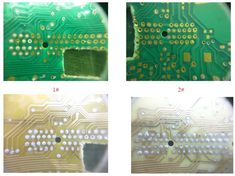
After the PCBA has been assembled,it usually needs to be wave soldered.In the wave soldering process,the tin permeability is very important,and whether the tin permeability is good or not has a direct impact on the reliability of the solder joints. If the tin permeability is not good after wave soldering,it is easy to cause problems such as virtual soldering. So how to solve the problem of poor tin permeability in wave soldering in PCBA processing?

Factors Affecting Wave Soldering Throughput
Wave soldering through the tin is mainly related to raw materials (PCB, components),wave soldering soldering process, the use of flux and manual soldering standards and other factors.
1.Raw material factors
Under normal circumstances after melting tin has a strong permeability,but not all metals can be penetrated, such as aluminium, aluminium metal surface will form a dense layer of protection, its molecular structure of other molecules is very difficult to penetrate into. In addition, if the surface of the metal has oxidation,tin is also difficult to penetrate into,the need to use flux treatment,or to clean up the oxide layer.
2.Wave soldering process factors
Poor tin permeability and wave soldering process is closely related to the need to reset the optimisation of soldering parameters,such as:wave height, temperature settings, soldering time and moving speed. The angle of the track can be appropriately lowered,the height of the new crest,improve the contact surface of the solder liquid and the pad and then properly adjust the wave soldering temperature, the higher the soldering temperature, the stronger the tin penetration, but the soldering temperature should be in the temperature range of the components can withstand and finally reduce the speed of transport,the new warm-up and soldering time, so that the flux can be fully removed from the surface of the oxides,penetrate the soldering joints to increase the rate of tin penetration.
3.Flux factors
Surface oxides,and to prevent re-oxidation during the soldering process,improper flux selection,uneven spraying,using too little or too much will lead to poor tin penetration.First of all,we should choose the right brand of flux,the effect will be better,in addition to regular inspection of the flux nozzle,to prevent clogging or damage to the nozzle.
4.Artificial soldering factors
In the wave soldering quality inspection,a part of the component is only the surface of the weld to form a cone,and the through-hole is not through the tin, the formation of virtual welding. Similar problems generally occur in manual soldering, mainly because the temperature of the welding is not enough or the welding time is too short.Poor wave soldering tin pass can easily lead to a weak soldering, thus increasing the cost of manual rework. Selective wave soldering tin permeability is much better than wave soldering,if the product has high requirements on soldering quality and tin permeability,you can use selective soldering, which can reduce the problem of poor tin permeability to a certain extent.
5.Wave soldering tin permeability requirements
Solve the problem of poor tin permeability
1.Preheat temperature 90-130℃,upper limit for more components,tin wave temperature 250+/-5℃,soldering time 3-5S.
2.The aperture of the mounting hole is 0.15-0.4mm larger than the diameter of the pins;take the lower limit for small pins and the upper limit for thick pins.
3.The pad size and pin diameter should be matched to facilitate the formation of the crescent surface.
4.Reflected to the PCBA processing plant to improve processing quality.
5.PCBA climbing angle of 3~7 ℃.
Wave soldering solder joints through the tin should generally reach more than 75%,that is,the panel appearance inspection tin rate should be higher than 75% of the thickness of the board,tin rate of 75% -100% can be.Wave soldering in the soldering heat by the PCBA suction fast,if the temperature is not enough out of the calamity will appear through the tin bad.In order to let PCBA get more heat,you can adjust the corresponding tin depth according to different PCBA.