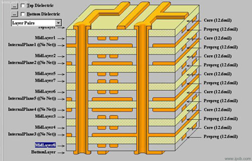
Laminate substrates are essential components of modern electronic devices. Commonly referred to as multilayer printed circuit boards (PCBs), they are widely used in a variety of applications, including smartphones, personal computers, and automotive electronic systems. This article will provide a detailed introduction to the basic concepts, manufacturing processes, characteristics, and advantages of laminates. Even beginners in electronic engineering will find this information useful.
Multilayer Laminate Substrates Overview
Laminate substrates are circuit boards composed of alternating layers of insulating and conductive layers (primarily copper foil). Generally, boards with two or more conductive layers are called multilayer boards, while boards with three or more conductive layers are called multilayer laminates. Compared to single- and double-sided boards, laminates allow for higher wiring density and accommodate more complex circuit designs.
The substrate for these circuit boards is typically a glass-reinforced epoxy resin (such as FR-4). The base material is a copper-clad laminate (CCL), and multiple layers of CCL are laminated together to enhance strength and functionality. During the lamination process, prepreg (a semi-cured resin sheet) is used as an adhesive to ensure insulation between layers.

Laminate substrates
Laminate Substrate Manufacturing Process
The manufacturing of laminate substrates involves multiple precision steps. Below, we'll explain the general manufacturing process step by step. The exact process may vary depending on the manufacturer, but the basic process remains the same.
Design Data Editing (CAM)
We convert the circuit design data provided by the customer into manufacturing data. We use computer-aided manufacturing (CAM) tools to optimize the wiring pattern and hole placement and check for manufacturability. Any defects will be repeatedly corrected.
Material Cutting
Copper-clad laminates and prepregs are cut to size. Inner and outer layer materials are prepared and handled in a clean environment.
Inner Layer Circuit Formation
Lamination (Dry Film Application): A photosensitive resist (dry film) is applied to the circuit board.
Exposure and Development: After the circuit pattern film is applied, it is exposed to UV light, and then a solvent is used to remove the unexposed areas.
Etching and Stripping: Chemicals are used to dissolve the exposed copper foil and remove unwanted areas. The resist is then stripped off, completing the inner layer circuitry. This process is repeated for multiple layers of inner layer boards.
Lamination (Layering and Pressing)
Prepreg is sandwiched between the inner layers, with copper foil placed on the outside and stacked. A vacuum press applies high temperature and high pressure to bond the layers together. This process is the core of lamination, as interlayer adhesion determines the quality of the board. Surface roughening (using, for example, black oxide) enhances adhesion.
Drilling
Vias in the connection layers and component mounting holes are drilled using high-precision CNC drilling machines, capable of producing thousands of holes at a time.
Copper Plating
Copper is plated on the inner walls of the holes to ensure interlayer conductivity. A combination of electroless and electrolytic plating achieves uniform film thickness.
Outer Layer Circuit Formation
Similar to the inner layers, the outer layers are patterned through lamination, exposure, development, and etching.
Solder Mask
Insulating ink is used to protect the circuitry. Exposure and development remove unwanted areas, leaving only the areas requiring soldering exposed.
Surface Treatment
Exposed copper areas are plated with gold or organic overcoat (OSP) to prevent oxidation and improve connectivity.
Contour measurement and inspection
Cut the circuit board to its final shape (milling). Conductivity checks and visual inspections are performed to eliminate defective products. Quality is confirmed through AOI (automated optical inspection) and electrical testing.
These processes are performed in a cleanroom and require strict control, as even tiny dust particles and temperature fluctuations can affect quality.
Features and Advantages of Laminate Substrates
High-density wiring: Multilayer structures enable complex circuits to be built within limited spaces, contributing to the miniaturization of electronic devices.
Noise reduction: Ground and power planes are located on inner layers to reduce signal interference.
Durability: Layering increases strength, making it resistant to vibration and heat.
Disadvantages: Manufacturing costs are high, and design errors are difficult to correct, but these issues are being improved with technological advances.
Advanced technologies such as build-up (using laser vias) are enabling further miniaturization of laminate substrates, driving their use in 5G communications and AI devices.
Laminates are a foundational technology in the electronics industry. Understanding the manufacturing process is crucial for designers and engineers and is key to producing high-quality products. In the future, we look forward to the development of flexible laminate substrates and environmentally friendly materials. If you have any questions, please leave a message!