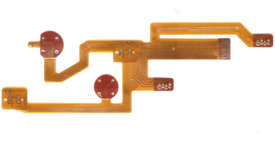
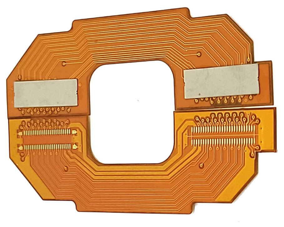
What are the advantages and disadvantages of FPC circuit board layout? Here is a brief introduction.
FPC (Flexible Circuit Board) is a type of PCB, also known as FPC. FPC is made of flexible materials such as polyimide or polyester film substrates, which have high wiring density, light weight, thin thickness, flexibility, quality advantages, and sensitivity to accept millions of dynamic bends without breaking wires. It can be moved and scaled freely according to spatial layout to complete 3D assembly and achieve the integration of components and wire connections. The advantages of circuit boards cannot be compared to other categories.
Advantages of FPC: The use of FPC can greatly reduce the volume and weight of electronic products, making it suitable for high-density, miniaturized, and high reliability directions of electronic products. Therefore, FPC is widely used in aerospace, military, mobile communication, portable computers, computer peripherals, PDAs, digital cameras and other fields or products. In addition, it can be organized according to spatial layout requirements, moved and flexible in three-dimensional space, thus achieving the integration of component installation and wiring
FPC disadvantage: Cost should be the most important consideration in the production process. Due to the fact that FPC circuit boards are designed and manufactured for special purposes, the initial cost of circuit planning, wiring, and circuit boards is relatively high. Unless there is a special need to use FPC, it is generally recommended not to use it several times. In addition, since a lot of effort has been invested in it, later maintenance is naturally necessary, so soldering and rework require trained personnel to operate.

FPC
Suggestions on FPC design
1. The PI thickness of FPC material is 12.5um. If a 25um PI is selected, the FPC will be too hard and the bending efficiency will be poor.
2. Copper thickness: generally 18um (1/2oz) is used.
3. All exposed copper areas must be gold-plated and nickel plated, with a thickness of 2-5 μ m for Ni and 0.1~0.2 μ m for Au. Gold plating is used to prevent oxidation. If it is too thin, the gold plating process is difficult to control and the anti oxidation effect cannot be achieved well. If it is too thick, it will affect the welding efficiency. The coating is too thick and prone to breakage during welding. For FPC used to connect external programs, due to the high number of insertions and removals, the thickness of the gold plating can be appropriately increased In order to achieve complete adhesion, the thickness of the adhesive should be slightly thicker than the PI layer. For example, a 12.5um PI can use a 20um adhesive.
4. The thickness of the reinforcing plate (including double-sided tape): commonly used are 0.1mm, 0.15mm, and 0.2mm. FPC dimensional tolerance and limit dimensions. External dimensional tolerance: ± 0.2mm.
5. Relative external tolerance of protective film window opening: ± 0.30mm. Hole diameter and bit of protective film window opening: ± 0.10mm. Limit tolerance of wire line width: line width ≥ 0.15mm, tolerance is ± 0.05mm, line width ≤ 0.15mm, tolerance is ± 0.03mm. Length dimension tolerance of gold finger: ± 0.30mm for external shape.
6. Installation holes, through-hole diameters, and hole bit sizes on FPC: ± 0.10mm.
7. The line edge distance of FPC is ≥ 0.2mm, and the relative dimensional tolerance between the mounting holes, through holes, and wires on FPC is ± 0.20mm The relative dimensional tolerance between the reinforcing plate and the outer shape is ± 0.3mm FPC thickness tolerance: ± 0.03mm
8. The minimum aperture of the gap hole in the FPC steel mold can reach 0.50mm. To prevent hole breakage, a minimum margin of 0.4mm should be left for the hole edge. The minimum aperture for CNC drilling is 0.20mm (such as metalized holes on solder pads).
9. For the convenience of suppliers to arrange testing, it is recommended that the FPC connector pad length be ≥ 0.90mm.
10. In order to ensure welding quality, the PITch value of the I/O port at the soldering end of a regular double-layer FPC should be ≥ 0.80mm, and the pad width should be ≥ 0.50mm.
11. The thickness of single-layer FPC is generally marked as 0.10 ± 0.05mm, and the thickness of double-layer FPC is generally 0.15 ± 0.05mm.
12. The general size tolerance of FPC is 0.2mm, and important size tolerances should be strictly controlled. In addition to size, if necessary, tolerances should be increased, such as tolerances for some positioning holes, width of solder pads, PITch values, length of electrodes connected to LCD, and PITch values. For some dimensions that do not require strict control, the tolerance can be relaxed, such as the positioning tolerance of some double-sided tape and the size of double-sided tape, which can be relaxed to ± 0.5mm. If it is a reference size, add parentheses to indicate it.
13. FPC positioning marks should generally not be marked with silk screen printing. If the error of silk screen printing marks is too large, the positioning marks should be made into solder pads.
14. FPC mechanical holes, and pay attention to controlling their tolerances, generally within ± 0.10mm. In order to improve efficiency, it is best to make positioning holes instead of positioning pads where multi-layer FPC is soldered.
15. When designing the alignment marks for FPC and LCD, it is advisable to ensure that the distance between the alignment marks on both sides of the FPC is at least 13mm, so that the camera can simultaneously illuminate the electrodes on both sides. Additionally, the mark can be a single electrode or a horizontal solder pad added to the nearest electrode.
16. Determine whether to choose high temperature resistant materials based on customer information input. If high temperature resistant materials are selected, the temperature that the reinforcing plate needs to withstand and the time at that temperature should be indicated in the annotation column. For example, white PET cannot be reflow welded, while reddish brown polyimide is the high temperature resistant material.
17. When drawing the outline of an FPC, it is generally required to draw three views: the front view, the back view, and the side view. The side view should describe the side profile of the FPC as detailed as possible, paying attention to the direction of the view and indicating the connection and welding surfaces Double layer FPC outline design.
18. FPC bending area design: The FPC bending area should be as soft as possible. In the external drawing, the bending area should be marked. In the bending area, there is usually only a single layer of wiring, so the PI layer and copper layer on the side without wiring can be removed to increase flexibility (the bent area in Figure 1 is the bending area). No vias, components, or solder pads can be placed within the bending area.
19. Requirements for the bending conditions of double-layer FPC: After the hot pressing and dispensing process is completed, bend 180 degrees along the bending direction, and the required number of bends is greater than 20 times.

FPC
20. Design of PI layer (reinforcement layer) on the back of FPC bending area: In order to achieve better hot pressing effect and strengthen the strength of FPC hot pressing end, a PI layer (reinforcement layer) needs to be added on the back of the hot pressing end electrode. The hot pressed end electrode needs to be bent after being hot pressed on the LCD, which can easily cause a fault between the bent area and the hot pressed end electrode. When bending the FPC, concentrated stress is generated between the bent area and the hot pressed end electrode, which can easily cause electrode breakage. Therefore, the PI layer on the back of the hot pressing end and the electrode on the hot pressing end must be staggered.
In the side view, the simple structure of the board should be drawn, indicating the position of the window. It should be clearly stated that there should be no exposed copper on the top of the window, and the distance from the top of the gold finger to the edge of the FPC should be ≥ 0.30mm. (Currently, some Chinese suppliers require testing wires for hollow FPC to be led out from the top, and copper must be exposed on the top. In this case, sufficient space should be left on the PCB to ensure that the exposed copper on the top of the hollow FPC is far away from the component area, and to prevent short circuits caused by copper exposure on the top of the window.). To prevent the golden finger from breaking, the length of each side of the golden finger beyond the window should be ≥ 0 30mm, the upper and lower windows can also be staggered, with a large window on the welding end and a small window on the bottom, with a displacement of 0.2mm on each side. To prevent hole breakage, the edge distance of the positioning hole and the distance from the hole to the window should be ≥ 0 40mm, if there are no special requirements, the positioning hole is generally made of non-metallic material and marked with (npth). The distance between the window and the top is ≥ 0.80mm. The I/O pad PITch of the FPC connected to the LCD through hot pressing on the multi-layer FPC should be consistent with the PITch on the FPC, but the pad width should be slightly larger than that of the FPC, and the upper end should exceed 0.3-0.5mm, and the lower end should exceed 0.2-0.3mm, so that it is easier to align during soldering.
21. The FPC grounding pad should be plated with Au, with a thickness of 0.075um to 0.125um.
22. When determining the shape of FPC, try to consider whether the component area is suitable as much as possible. There should be sufficient wiring space and meet the functional requirements of the circuit. Especially when marking the dimensions of the mold opening diagram for anti-static and EMI, edge positioning and center symmetry marking methods are usually used. For mold drawings with irregular shapes or slots or openings that are not symmetrical about the center, the edge positioning method can be used to indicate dimensions. For other mold drawings that are symmetrical about the center, the center positioning method or edge positioning method can be used to indicate dimensions. However, it is best to mark the mutual position between the I/O ports on both ends of the FPC to avoid misalignment caused by excessive positioning tolerance of the FPC edge, which may result in assembly failure.
23. After hot pressing the FPC onto the LCD, in order to prevent the FPC from breaking, it is best to press the 0.20mm PI onto the step. If the flexible board does not need to be bent, the PI can be designed without the step,