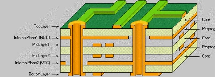
First of all, a four-layer PCB is composed of four layers, including: top layer, bottom layer, signal layer (inner layer 1), power/ground layer (inner layer 2)
1. Top Layer
The top layer is the topmost layer of a four-layer PCB. It is the layer connected to external components, also called the signal layer or the surface layer. The top layer is usually used for the layout of components and circuit connections to form traces, as well as the setting of regional test points. The base material of the PCB is glass fiber, and the first layer is the bottom layer of glass fiber. Its main function is to carry the PCB board and is the supporting structure of the entire circuit board. In addition, it can also isolate and protect the circuit board so that the signal of the circuit board will not be interfered with by external interference, noise, etc.

four-layer PCB
2. Bottom Layer
The bottom layer is the bottom layer of a four-layer PCB. It is the layer where the PCB board contacts the bottom of the installed device, also called the ground layer or bottom layer. The bottom layer is usually used for routing, grounding facilities and installation of components in the earth area.
3. Signal layer (middle inner layer 1)
The signal layer is the middle layer of the four-layer PCB, which is separated from the top and bottom layers by a power/ground layer. It usually includes inner layer 1 and its connection layer. It is the main signal layer of the circuit board. Therefore, blind holes and blind buried holes are usually required to connect the upper and lower signal layers. The signal layer is generally used for the connection of long topological paths and multi-layer circuits, which makes it difficult to achieve single-sided boards. It can also provide pressure for the support of large-size PCB boards.
The second layer is the internal layer, which we also call the GND layer, which is the layer used for grounding. In the design of PCB boards, the GND layer occupies an important position. It can shield electromagnetic interference and prevent signal reflection. At the same time, it can also play an excellent battery role in the entire circuit board.
4. Power/ground layer (middle inner layer 2)
The power/ground layer is the middle layer of the four-layer PCB for wiring or filling power/ground, also called the power layer (Power Layer) or ground plane layer (Ground Plane Layer). It is mainly responsible for controlling electromagnetic interference radiation (EMI/EMC) waves, increasing the anti-interference ability of the signal layer, and effectively preventing cross-coupling, signal crosstalk, etc. The power layer is usually divided into a positive power layer and a negative power layer. If a double-layer PCB is used, there is only one ground plane.