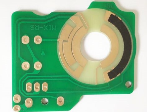
A single layer pcb board is the most basic type of printed circuit board. The substrate has only one side covered with a conductive layer (usually copper), used to support and connect components. It has a simple structure and low cost, making it suitable for simple electronic products with single functions and large production volumes, such as calculators, LED lighting, and home appliances.
Typically, a single layer pcb board consists of the following parts:
Substrate
Commonly uses FR-4 (glass fiber reinforced epoxy resin), CEM-1, or CEM-3 as the support material, providing mechanical strength and insulation.
Conductive Layer (Copper Layer)
The conductive traces of a single-layer board are usually etched from copper foil, with a thickness of typically 1oz (approximately 35 µm), which can be increased to 2oz or thicker depending on requirements.
Solder Mask
Protects the circuitry, prevents solder short circuits, and enhances the durability and aesthetics of the board.
Silkscreen Layer
Used to mark component numbers, identifiers, and other information for easy assembly and inspection.

single layer pcb board
What are the characteristics of a single layer pcb board?
Easy to design and manufacture: The design and manufacturing complexity of single-layer PCB boards are relatively low, resulting in much shorter delivery times compared to other types of PCBs. Single layer pcb boardcan be delivered within two weeks, and the delivery time can be further shortened with expedited service. The probability of defects in single-sided circuit boards is much lower than that of double-sided and multi-layer PCBs.
The manufacturing process of single layer pcb board is relatively simple: the solder mask and screen printing processes are not complex, reducing the number of steps and thus shortening production time;
Cost-effective: Because the PCB only needs to be assembled on one side, single layer pcb boards have the lowest cost among other PCB categories. Similar to manufacturing, single layer pcb boards only require processing one conductive layer, requiring fewer steps. Similarly, in terms of assembly, single layer pcb boards only have components on one side, reducing processing time and the number of components and materials that need to be purchased.
Easy to repair: If manufacturing and assembly defects occur, single layer pcb boards have the advantage of being easy to repair. This means that rework and repair have minimal impact on the functionality of the printed circuit board. This is because there are fewer components and traces in a single-sided circuit board that could interfere with the repair process.
Applications of single layer pcb boards:
Low-Cost Electronic Products
In low-cost fields such as home appliances, toys, and lighting, single-layer boards remain irreplaceable.
Education and Prototyping
Due to their low learning curve and simple manufacturing process, single-layer boards are still commonly used in electronics education and development boards.
Smart Manufacturing Upgrades
Automated production and high-precision etching technology will make single-layer board production more efficient and environmentally friendly.
Miniaturization and Modularization
single layer pcb boards, when combined with other modules, can still achieve functional integration, meeting the needs of certain specific applications.
Design Considerations for single layer pcb boards:
Reasonable Wiring
Avoid line crossings and long-distance routing to improve signal integrity.
Component Layout Optimization
Distribute heat-generating components reasonably to reduce interference and improve heat dissipation.
Size Control
To reduce costs, minimize the PCB area while still meeting functional requirements.
Selection of Appropriate Materials
Choose appropriate substrate and copper thickness based on the working environment and current carrying requirements.
Testing and Verification
Although single layer pcb boards are simple, electrical testing is still necessary to ensure there are no short circuits, open circuits, or other problems.
Production Process of single layer pcb boards:
The production process of single layer pcb boards is relatively simple, but every step is crucial to ensure the quality and reliability of the final circuit board. The entire process starts with PCB layout design, followed by copper-clad laminate cutting, surface treatment, circuit printing, etching, drilling, silkscreen printing, solder mask application, and finally shaping, inspection, and packaging. Each step requires strict control of process parameters and operational details. For example, the board material needs to be baked before cutting the copper-clad laminate, the surface must be free of dust and burrs during the grinding process, the ink used for circuit printing must have anti-corrosion properties, the circuit ink must be thoroughly cleaned after etching, and attention must also be paid to drying and precise positioning during the solder mask and silkscreen printing processes. Through these steps, single-layer boards can be produced at low cost and high efficiency while ensuring electrical performance and reliability.

single layer pcb board
The production of single layer pcb boards mainly includes the following steps:
Designing the PCB Layout
Use CAD software to design the circuit schematic and convert it into a PCB layout diagram, determining the wiring path and component positions.
Photoengraving
Transfer the designed PCB pattern onto the copper-clad laminate using a photolithography process. Etching:
Using a chemical solution to remove excess copper foil, leaving only the designed circuit traces.
Drilling:
Drilling holes for component pins or mounting holes. Single-layer boards only require simple through-holes and do not involve double-sided interconnections.
Plating and Coating:
To improve soldering performance, the circuit surface is usually plated with tin or gold and coated with a solder mask to protect the traces.
Screen Printing and Testing:
Screen printing component numbers and markings, and performing electrical testing and visual inspection to ensure the PCB is qualified.
Cutting and Packaging:
Cutting the finished PCBs to size and packaging them for shipment.
Due to the significant advantages of single layer pcb boards in terms of cost and ease of design, manufacturing, and assembly, this type of circuit board remains an ideal choice for many applications. In many electronic devices we use daily, single layer pcb boards form the foundation for numerous components, enabling the devices to function properly. Even with the emergence of more complex types such as multi-layer boards, single layer pcb boards still play an important role in low-density electronic products.