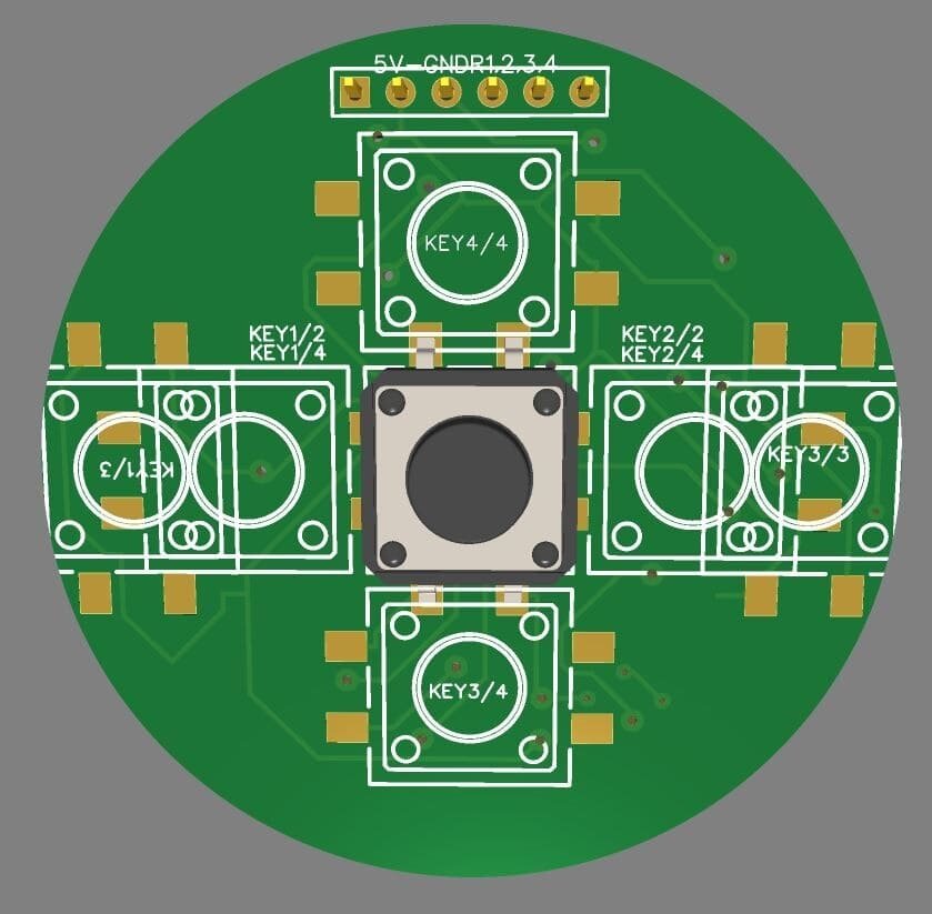
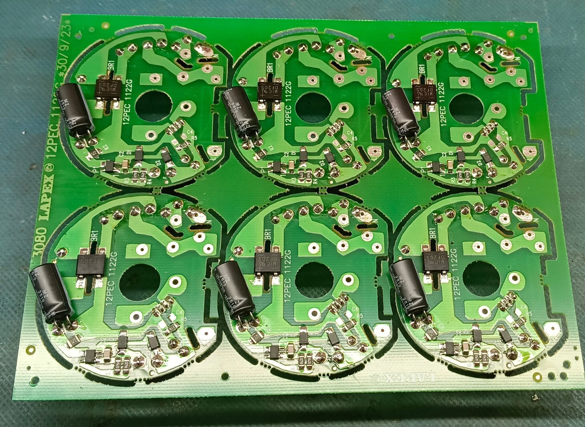
In most people's minds, PCBs are usually regular rectangles or squares: neat, rational, and easy to arrange. As technology becomes smaller and more creative, circular PCB boards are becoming increasingly popular. Compared to common square and rectangular PCBs, the biggest difference of circular PCB boards lies in their shape, but their basic principles, materials, and manufacturing processes are the same. They can also be made into single-layer, double-layer, or multi-layer boards. Simply put, when the casing or internal structure of an electronic product is circular, curved, or symmetrical, a circular PCB is more suitable, allowing for better space utilization and a more compact and stable product structure.

circular PCB boards
Typical Application Scenarios of Circular PCB boards
Although circular PCB boards will not replace traditional PCBs, in some specific areas, they are often a more suitable choice.
1. Wearable devices: such as smartwatches and health monitoring devices. Circular PCB boards are easier to fit into the casing structure, allowing for a more compact layout in a limited space, while also improving stability during wear.
2. LED lighting: circular light boards, downlights, panel lights, etc. The circular structure facilitates the even arrangement of LEDs and, combined with an aluminum substrate, achieves better heat dissipation.
3. Sensors and industrial modules: such as gas sensors and environmental monitoring equipment. Circular PCB boards facilitate sealed designs, suitable for long-term stable operation in industrial applications.
4. Audio equipment: microphone modules, speaker control boards, etc. Circular PCB boards better meet acoustic structure requirements, helping to save space and optimize the internal layout.
5. Smart home devices: rotary controllers, circular panel devices. Circular PCBs meet functional requirements and provide more flexibility for product appearance design.
The common characteristics of these products are: limited space, special structure, and certain requirements for stability and appearance design.
Advantages of Using Circular PCB boards
1. Higher Space Utilization
Circular PCB boards can perfectly match circular or curved casing structures, especially suitable for products with limited volume such as smartwatches, LED lighting, and sensors. Compared to traditional square PCBs, the circular design reduces wasted corner space, making the internal layout more compact and reasonable, which helps to improve overall integration.
2. Beneficial for Reducing Electromagnetic Interference (EMI)
Because circular PCBs do not have sharp right angles, the wiring turns are smoother, which can reduce signal reflection and electromagnetic interference to a certain extent. This is especially important in high-frequency or high-density circuits, contributing to improved device stability.
3. Improved Signal Integrity
Circular PCB boards make it easier to maintain consistent trace lengths and impedances during layout and routing, facilitating stable transmission of high-speed signals, reducing signal loss and crosstalk, and thus improving overall electrical performance.
4. Superior Heat Dissipation Performance
In LED and power applications, circular PCBs (especially aluminum substrates) help to evenly dissipate heat in all directions, improving heat dissipation, reducing localized overheating problems, and thus extending the lifespan of the PCB and components.
5. Stronger Reliability and Adaptability
The stable structure of circular PCBs and more even stress distribution make them more reliable in vibrating or complex environments. At the same time, their design can be customized according to different application needs, adapting to various industry scenarios.
6. Balancing Aesthetics and Cost Advantages
Circular PCBs better meet the aesthetic requirements of modern consumer electronics products, appearing simpler and more visually appealing. Combined with mature production processes and mass manufacturing methods, they can also achieve better cost control, offering excellent value for money.
Considerations in Circular PCB Design:
1. Wiring Area Division: Clearly divide the wiring areas for digital, analog, and DAA signals to avoid signal interference.
2. Signal Trace Length: High-speed digital signals and sensitive analog signals should have the shortest possible traces to reduce signal attenuation and interference.
3. Power and Ground Plane Layout: Power and ground lines should be arranged radially as much as possible to reduce signal loops and improve anti-interference capabilities.
4. Wiring Density and Order: Start wiring from the area with the most complex connections or the highest wiring density, following the principle of prioritizing critical signal lines.
5. Wiring Angle and Direction: Traces should preferably use 45° angles, avoiding 90° right angles, and inter-layer wiring directions should be perpendicular to reduce interference.
6. Pad and Via Design: Pad design should consider component mounting requirements, and vias should be reasonably placed to connect signal lines on different layers.
7. Critical Signal Protection: Critical signals such as power, small analog signals, and high-speed signals should be surrounded by ground planes to enhance their anti-interference capabilities.
8. Wiring Spacing and Width: Reasonably set wiring spacing and width according to signal type and current requirements to ensure signal transmission quality.
In the manufacturing of circular PCBs, panelization is a particularly important aspect that requires careful attention. Compared to square boards, circular boards cannot utilize the low-cost, high-efficiency V-CUT depaneling method due to the absence of straight edges. This presents certain challenges in panel design. Therefore, when designing circular PCBs, it is necessary to optimize the overall structure by considering details such as wiring layout, signal protection, and power and ground plane arrangements to ensure that each circuit board maintains good performance and reliability during panelization, assembly, and use.
Common Panelization Methods:
Perforated Holes + Bridging
A row of small holes (perforated holes) is designed between adjacent circular PCBs, and connected with small copper or substrate bridges to maintain overall strength. This method is low-cost and easy to process, but the edges may have slight burrs after depaneling, requiring post-processing or acceptance if edge requirements are not stringent. The size of the bridges and holes needs to be designed appropriately to ensure panel strength and that component layout is not affected.
Milling Slots
Using a CNC milling machine to mill narrow slots between the boards results in smooth and neat edges after depaneling, with high appearance quality. Complete cutting or retaining a thin layer is possible, but the cost is higher than the perforated hole method, and the milling path design is more complex. The slot width, path, and residual thickness need to be precisely controlled to ensure smooth depaneling and panel strength.

circular PCB boards
Panel Layout Methods:
Rectangular Array Arrangement: Circular PCB boards are arranged in a regular rectangular array. This layout is simple and has high material utilization, making it the most commonly used method.
Staggered Arrangement: Circular PCBs are arranged in a staggered pattern, resulting in higher material utilization. However, the panel shape is complex, and the milling and bridging design is more difficult and costly. This method is usually only used when the quantity is large and cost pressure is high.
Circular PCB Panelization Notes:
Process Edges and Mark Points: Circular boards do not have straight edges. Process edges are used for guide rails, clamping, and optical positioning, and mark points are used for SMT assembly accuracy. They must be reasonably arranged to ensure accurate assembly and depaneling.
Reinforcing Ribs and Residual Thickness: These increase panel rigidity and prevent bending during transportation or production.
Depaneling Instructions: Mark "Cut Here" at the perforated hole or milling slot locations to ensure that operators clearly understand where to depanel.
Circular PCB boards are becoming increasingly popular in modern electronic products. Compared to square boards, circular PCBs offer significant advantages in terms of space utilization, signal integrity, heat dissipation, and aesthetic design. However, they also present challenges in manufacturing and panelization, such as the inability to use V-cut depaneling, requiring alternative methods like stamp holes with bridging or milling slots. Details such as panel layout, process edges, fiducial marks, and stiffeners directly impact production efficiency and assembly quality. Therefore, these factors must be carefully considered during the design phase, and close communication with the manufacturer is crucial. As a professional PCB manufacturer, iPCB possesses extensive experience in circular PCB boards production and can provide a one-stop service ranging from design guidance and panel optimization to mass production, helping customers efficiently and reliably complete their circular PCB boards projects and achieve optimal performance and aesthetics.