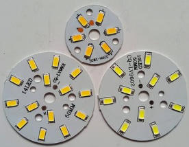
In modern electronics, the diode substrate is not only a decisive factor in diode performance but also directly impacts the stability and efficiency of the entire electronic system.
What is a diode substrate? Simply put, a diode substrate refers to the semiconductor substrate material used to manufacture diodes. It is typically composed of high-purity crystalline materials such as silicon (Si), gallium arsenide (GaAs), or gallium nitride (GaN). These materials provide a stable platform for doping and forming the PN junction—the core structure of the diode. The PN junction is key to achieving unidirectional conduction in a diode. By implanting different types of impurities (such as P-type and N-type dopants) into the diode substrate, forward conduction and reverse blocking characteristics are achieved.
Why is the diode substrate so important? Because it directly determines the diode's electrical performance, thermal stability, voltage withstand capability, and lifespan. For example, in high-power applications, if the diode substrate's thermal conductivity is insufficient, the device is prone to overheating and failure. According to semiconductor physics, the diode substrate's lattice structure must be perfect to minimize defect density, thereby reducing leakage current and improving efficiency. According to the Semiconductor Industry International (SEMI), high-quality diode substrates can increase diode conversion efficiency by more than 20%.

diode substrate
The development of diode substrates dates back to the mid-20th century. In 1947, Bell Labs invented the first transistor, laying the foundation for modern diode substrates. Early diode substrates primarily used germanium (Ge), but due to its narrow bandgap (approximately 0.66 eV) and poor high-temperature resistance, it was quickly replaced by silicon. Silicon, with its bandgap of 1.12 eV, is low-cost and easy to process, becoming the mainstream choice.
In the 1980s, with the rise of compound semiconductors, diode substrates entered an era of diversification. Gallium arsenide diode substrates flourished in optoelectronic devices due to their direct bandgap properties, which are suitable for laser and LED applications. In the 1990s, Nakamura Osamu, the inventor of the blue LED, and others used gallium nitride diode substrates to achieve high-efficiency light-emitting diodes. This technology was recognized with the 2014 Nobel Prize in Physics. In recent years, with the rise of 5G and new energy vehicles, silicon carbide (SiC) and gallium nitride diode substrates have become popular. These wide-bandgap materials (bandgaps exceeding 3 eV) can withstand higher voltages and temperatures, making them suitable for power electronics.
Technological advances are also reflected in crystal growth methods. The traditional Czochralski (CZ) method is used for silicon diode substrates, while molecular beam epitaxy (MBE) and metal-organic chemical vapor deposition (MOCVD) are used for compound diode substrates. These methods ensure atomic-level flatness of the diode substrate, with defect densities kept below 10^3 per square centimeter.
The choice of diode substrate material depends on the application requirements. Common types are as follows:
Silicon substrates: The most common choice, accounting for over 70% of the market share. Advantages include low cost, mature processes, and good mechanical strength. Disadvantages include a narrow bandgap, making them unsuitable for high-frequency or high-temperature environments. In Schottky diodes, silicon diode substrates are often used for power rectification.
GaAs substrates: High electron mobility (approximately 8500 cm²/V·s, five times higher than silicon) makes them suitable for RF and optoelectronic applications. For example, in PIN diodes for solar cells, GaAs diode substrates achieve higher power-to-electricity conversion efficiencies (over 25%).
GaN substrates: An emerging star, with a bandgap of 3.4 eV and high thermal conductivity (approximately 200 W/m·K). Its use as diode substrates in power amplifiers and electric vehicle chargers can reduce energy loss by 30%. However, GaN diode substrates are difficult to grow and expensive, and are currently dominated by companies such as Cree and Osram.
Silicon carbide substrates: They are resistant to high temperatures (up to 600°C) and have a high breakdown voltage (approximately 3 MV/cm). In high-voltage diodes such as SiC Schottky diodes, these substrates are widely used in wind power and high-speed rail systems.
In addition, emerging materials such as diamond diode substrates offer thermal conductivity as high as 2000 W/m·K, but due to complex processing, they are still in the laboratory stage. Material selection must consider parameters such as bandgap, electron saturation velocity, and thermal expansion coefficient to match the specific diode type.
The process for manufacturing diode substrates is highly precise and typically includes the following steps:
Crystal growth: Single crystal ingots are grown using the CZ or float zone method and then sliced into thin wafers (approximately 0.5-1 mm thick).
Surface treatment: Chemical mechanical polishing (CMP) is used to achieve nanometer-level surface flatness on the diode substrate surface. Doping and Epitaxy: An epitaxial layer is deposited on the diode substrate and implanted with boron (P-type) or phosphorus (N-type) impurities to form a PN junction.
Photolithography and Etching: Patterns are defined using photolithography techniques, followed by etching of the electrode contact areas.
Testing and Packaging: Electrical testing is performed on the diode substrate to ensure a forward voltage drop of less than 0.7V and a reverse leakage current in the microampere range.
The entire process must be performed in a cleanroom to avoid the introduction of contaminants. Advanced manufacturers such as Intel and TSMC utilize EUV lithography to further enhance the integration of diode substrates.
Diode substrates are used in every aspect of our daily lives. In consumer electronics, silicon diode substrates are used as rectifier diodes in mobile phone chargers, ensuring efficient energy conversion. In the lighting sector, GaN diode substrates drive LED light bulbs, with the global LED market exceeding $50 billion.
Diode substrates will continue to evolve towards higher performance and lower costs. Quantum dots and two-dimensional materials (such as graphene) may be integrated into diode substrates, enabling sub-nanometer devices. Sustainability is also a key concern, and technologies for recycling silicon diode substrates are emerging to reduce environmental impact. Diode substrates are the cornerstone of semiconductor technology, supporting the development of modern electronic civilization, from basic materials to advanced applications. Through continuous innovation, we can expect more efficient and reliable diode devices.