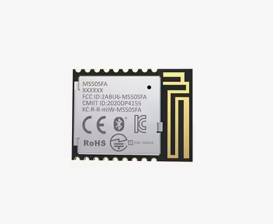
What is HF PCB? HF refers to high-frequency PCB, high-frequency electromagnetic frequency special circuit board, high-frequency frequency in 1GHz or more, its physical properties, precision, and technical parameters are very high, HF PCB is generally used in radar systems, satellites, antennas, cellular telecommunication systems - power amplifier and antennas, live satellites, E-band point-to-point microwave links, radio frequency identification (RFID) tags, airborne and ground radar systems, millimeter wave applications, missile guidance systems, space satellite transceivers and other fields.
HF PCB impedance control requirements are stringent, the relative line width control is rigorous, and the general tolerance is about two points or so; because of the special high-frequency circuit board board board, PTH copper sinking adhesion is not high, it is necessary to use plasma processing equipment to roughen the over-hole and the surface, to enhance the adhesion; high-frequency circuit boards are special circuit boards with high electromagnetic frequency.
When manufacturing HF PCBs, the dielectric loss (Df) is small, mainly affecting the quality of signal transmission. The smaller the dielectric loss, the smaller the signal loss; the lower the absorption rate, the higher the absorption rate, will affect the dielectric, and dielectric loss will be affected. The dielectric constant (DK) must be small and stable. Usually, the smaller the transmission speed of the signal, the better. The transmission rate of the signal is inversely proportional to the square root of the material's dielectric constant. A high dielectric constant tends to cause delays in signal transmission. HF PCB substrate dielectric constant (Dk) must be small and stable, generally the smaller the better, the transmission rate of the signal is inversely proportional to the square root of the material's dielectric constant, and a high dielectric constant tends to cause delays in signal transmission. As far as possible with the thermal expansion coefficient of copper foil, because inconsistency will lead to separation of copper foil in hot and cold changes; other heat resistance, chemical resistance, impact strength, peel strength, etc. HF PCB substrate water absorption should be low, high water absorption will be caused by moisture in the dielectric constant and dielectric loss.
Currently, the more commonly used HF PCB substrate is Teflon material, which is usually used above 5GHz. When manufacturing HF PCB, the commonly used boards are Rogers, ISOLA, Taconic, Panasonic, Taiyo, and domestic Wangling boards.

How to deal with some theoretical conflicts in the actual wiring of HF PCB?
It is right to separate analog/digital land. It is important to note that the signal routing should not cross the moat and that the return current path between the power supply and the signal should not be too large. Crystal is an analog positive feedback oscillator circuit, to have a stable oscillation signal, must meet the specifications of the loop gain and phase, and this analog signal oscillation specifications are very easy to interfere with, even if you add ground guard traces and may not be able to isolate the interference completely. And too far away from the ground plane noise will also affect the positive feedback oscillation circuit. Therefore, the distance between the crystal and the chip must be as close as possible.
High-frequency PCB above 2G belongs to RF circuit design, not within the scope of high-speed digital circuit design. The layout (layout) and wiring (routing) of RF circuits should be considered together with the schematic because the layout and wiring can cause distribution effects. Moreover, some passive components of RF circuit design are realized by parametric definition and specially shaped copper foils, therefore, EDA tools are required to provide parametric devices and edit specially shaped copper foils. boardstation of Mentor Company has a special RF design module, which can meet these requirements. Moreover, general RF design requires a specialized RF circuit analysis tool, the industry's most famous is Agilent's soft, and Mentor's tools have a good interface.
There are indeed many conflicts between high-speed cabling and EMI requirements. However, the basic principle is that the resistor-capacitor or ferrite bead added due to EMI cannot cause some electrical characteristics of the signal to be out of specification. Therefore, it is best to first use the arrangement of routing and PCB layering techniques to solve or reduce the EMI problem, such as high-speed signals in the inner layer. Finally, a resistor-capacitor or ferrite bead is used to minimize the damage to the signal.
With the rapid development of technology, equipment features are more and more complex, many devices are designed in the microwave band or even more than millimeter wave. This also means that frequencies are increasing and the requirements for circuit board substrates are becoming higher. As the frequency of the power signal increases the loss of the substrate material is required to be very small, so the importance of high frequency boards comes to the fore.