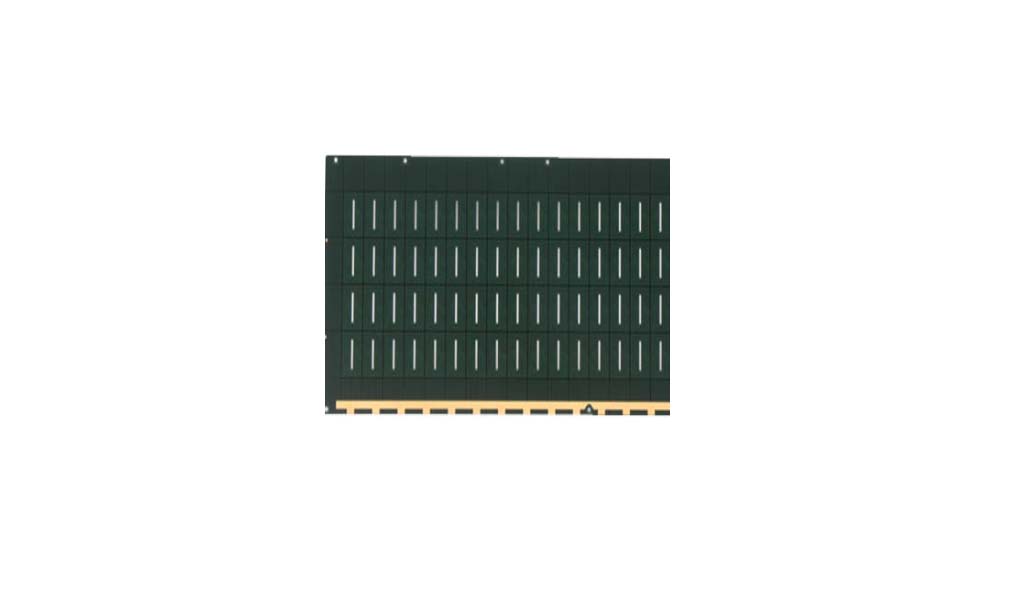
What is laminate substrate packaging? It is a semiconductor packaging process performed on a laminate substrate, such as solder ball connection, flip chip connection, wire bonding, and chip connection. Laminate substrate packaging uses a ball grid array (BGA) design to connect the chip to a plastic or tape laminate substrate, and the electrical connection is located at the bottom of the package.
Packaging designs such as plastic ball grid array (PBGA), flip chip ball grid array (FC-BGA), chip scale package (CSP), and package on package (PoP) are all laminate substrate packaging applications. A variety of technologies and materials are required to create highly reliable laminate packages. BGA packaging uses a matrix pin arrangement. Compared with traditional surface mount packaging, the package size of BGA packaging can be made smaller with the same number of pins, and it also saves more wiring area on the PCB board.
The term packaging has not been used in electronic engineering for a long time. In the era of vacuum tubes, mounting devices such as electron tubes on tube sockets to form circuit equipment was generally called assembly or assembly. At that time, there was no concept of packaging. Since the emergence of semiconductor components such as triodes and ICs, the history of electronic engineering has changed. On the one hand, these semiconductor components are small and delicate; on the other hand, they have high performance, and are multifunctional and multi-specification. In order to give full play to their functions, they need to be reinforced, sealed, and expanded so as to achieve reliable electrical connection with the external circuit and obtain effective mechanical support, insulation, signal transmission and other protection. The concept of "packaging" emerged on this basis.
Package Substrate is composed of electronic circuit carrier (substrate material) and copper electrical interconnection structure (such as electronic circuit, via, etc.), in which the quality of electrical interconnection structure directly affects the stability and reliability of integrated circuit signal transmission and determines the normal function of electronic product design function. Package substrate belongs to special printed circuit board, which is the basic component that connects high-precision chips or devices with low-precision printed circuit boards.

Inorganic substrates are mainly ceramic substrates, which have the characteristics of high thermal conductivity, high modulus, and low thermal expansion coefficient;
Organic laminate substrate packaging are usually used in 2.5D/3D, flip chip and system-level packaging (SiP). The devices of this type of package are located on the substrate. The material of organic substrate is usually FR-4 or other materials. FR-4 is a glass cloth composed of epoxy resin. These substrates use similar or the same materials as PCBs. So in some circles, organic substrates are sometimes called PCBs. Organic substrates are also multi-layer technologies, where at least two organic layers are separated by a metal layer. The metal layer acts as an electromigration shield in the package. Organic substrates have good electrical insulation, low dielectric constant, small mass, low manufacturing cost, and easy automation. Compared with inorganic substrates, organic substrates are more widely used.
Ceramic packages can be largely regarded as legacy technology. Although they were common in ICs in the past, they are now almost exclusively used in high-reliability applications such as military and avionics. Due to the reluctance to make changes in packaging technology.
Organic laminate substrate packages (BGA, CSP) use a small rigid (sometimes curved) substrate on which the die is wire bonded or flip-chip. Most such packages use a set of balls or grounds to interface with the host PCB. Which allows these packages to accommodate up to 4000 external I/0s!
The BGA format has advantages in lower thermal resistance, lower inductance, and increased number of interconnections. Therefore, laminate substrate packaging has wider applications in gate arrays, microprocessors/controllers, memory, analog, and RF devices.