The pcb board assembly process is the most critical step in developing any electronic product. This article will comprehensively introduce the process, key processes, required equipment and quality control points of PCB assembly to help readers gain a deep understanding of this core manufacturing link.
Following the PCBA process will ensure that the printed circuit board assembly process goes smoothly and produces the highest quality final product.
What is PCB board assembly?
PCB board assembly (PCBA) refers to the welding of electronic components according to design requirements on a bare board PCB (a circuit board without any components soldered) to make it a fully functional electronic circuit board. The process includes surface mount technology (SMT), plug-in (DIP), welding, testing, assembly and other links.

pcb board assembly process
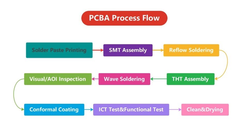
PCBA process flow
1. Solder paste printing
Solder paste printing is the first key step in the PCB assembly process. Its main task is to accurately print the right amount of solder paste on the specified pad area of the circuit board through the steel mesh. The type of solder paste needs to be selected according to the components and welding process used, and the size of the steel mesh opening must also strictly match the PCB drawing.
During the printing process, the solder paste is evenly applied by a scraper or metal blade so that the surface of the pad is covered with a solder paste layer of appropriate thickness, providing a basis for subsequent component mounting and welding.
2. SMD assembly
After the solder paste is printed, the surface mount component installation phase begins. In the past, most SMD work was done manually, but now it is mainly done automatically by the SMD machine.
The SMD equipment picks up various SMD components from the component packaging based on the pre-programmed position information, and accurately installs them to the solder paste-covered pad position through a vacuum nozzle or a fixture head. The whole process is fast and accurately positioned, greatly improving production efficiency and consistency.
3. Reflow soldering
After confirmation, reflow soldering will be performed. In reflow soldering, solder paste is first applied to the circuit board. Next, the component is placed in the correct position on the PCB, and then the component is heated by infrared radiation and convection. As the PCB is heated, the solder paste melts and reflows around the component leads and joints, forming a strong mechanical and electrical connection.
4. Inspection after reflow
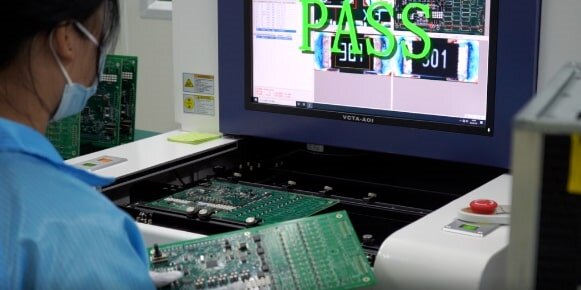
Automated optical inspection (AOI) after reflow
After the reflow process, we need to perform automated optical inspection (AOI) to check whether the continuous movement of the PCB during the reflow process has caused poor connection quality and component placement errors. These methods include manual inspection, AOI, manual inspection x-ray inspection (AXI), etc.
X-ray inspection of BGA
Soldering quality inspection for components with invisible solder joints such as BGA and QFN.
5. THT assembly
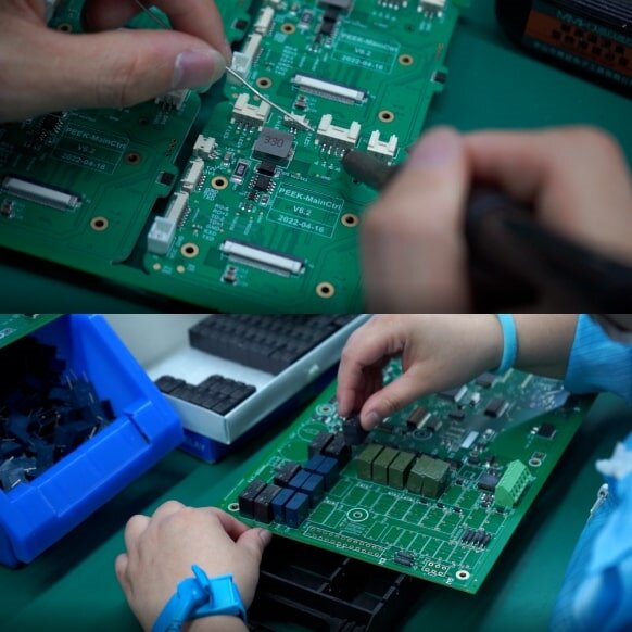
Some types of components need to be inserted into the PCB board, which is generally done manually.

6. Wave soldering
After the PTH components are inserted into the PCB and inspected, we will solder the components by wave soldering.
Wave soldering is an efficient and economical way to connect PTH components to PCBs. This process uses a wave of molten solder, which is applied to the PCB through a hot liquid solder tank. The hot solder will then flow into the PTH holes, and the component pins will be soldered to the PCB after cooling.
7. Visual/AOI Inspection
Inspections after wave soldering include visual inspection, AOI inspection, and tests to measure electrical characteristics such as continuity, voltage drop, and resistance. By performing these inspections regularly, manufacturers can ensure that their products will function properly after use.

8. Conformal coating
Some circuit boards are used in harsh environments (such as industrial control, automotive, military, etc.) and require three-proof treatment (moisture-proof, mildew-proof, and corrosion-proof).
9. Final inspection and functional testing
After all soldering steps are completed, the PCB will undergo final functional testing (FCT), which is an important part of evaluating whether the product is operating normally. The test simulates the actual use environment, powers on the circuit board and inputs signals, and detects key electrical characteristics such as voltage, current, and signal output.
If the test data exceeds the allowable range, the circuit board will be judged as unqualified. According to the standard, the problem board may be returned for repair or scrapped. Functional testing is a crucial step in pcb board assembly and directly determines whether the product can be delivered.
10. Post-cleaning process
During the assembly process, pollutants such as flux, dust and fingerprints will remain, which will not only affect the appearance, but may also corrode the solder joints for a long time and reduce reliability. Therefore, after all processes are completed, the circuit board needs to be thoroughly cleaned.
Usually, stainless steel high-pressure cleaning equipment is used, combined with deionized water for rinsing, which can effectively remove residues without damaging components. Compressed air is then used for rapid drying to ensure that the circuit board is neat and dry, ready for packaging and shipment.
PCB board assembly is a process of processing a PCB blank board through a series of processes, and finally processed into an electronic product that can be used by users. Any problem in any link will have a great impact on the quality of the product.