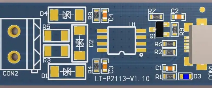
In the manufacturing process of PCB (printed circuit board), PCB silk screen may seem to be a subtle link, but it actually plays a vital role. It not only provides key information for subsequent production, debugging and maintenance, but also acts as an invisible guide on the circuit board, leading the smooth progress of each step.
1. Definition of PCB silk screen
PCB silk screen,full name Silkscreen Layer, also known as text layer or character logo layer, is a process of printing text, symbols, patterns and other information on the surface of PCB board by screen printing. These silk screen information are rich and varied in content and form, which can be letters, numbers, text, and even pictures, which provides great convenience for the production, debugging, maintenance and management of circuit boards.
2. Content of PCB silk screen
The content of PCB silk screen mainly includes the following aspects:
Component number: clearly indicate the location and name of each electronic component to facilitate accurate patching by production personnel.
Polarity identification: For components with polarity requirements, such as diodes, capacitors, etc., clearly indicate the positive and negative directions to avoid component damage or circuit failure due to installation errors.
Manufacturer logo and date code: provide a basis for product traceability and quality control. Sometimes, the company logo is also displayed through silk screen printing to increase brand recognition.
Test point and version number: Each test point has its name and location, which is convenient for debugging and maintenance; at the same time, the version number helps to distinguish different batches of circuit boards.

3. The role of PCB silk screen printing
Improve production efficiency: Workers can quickly and accurately install electronic components to the designated location based on the clear instructions of the silk screen, reducing the time for searching and confirming, and reducing the rate of manual errors.
Convenient for debugging and maintenance: Technicians can quickly locate faulty components and analyze circuit connection relationships based on silk screen markings, greatly shortening the time for troubleshooting and repair.
Product traceability and quality control: Through information such as manufacturer logos and date codes, the production source of the product can be traced back to provide strong support for quality control.
4. Quality requirements for PCB silk screen printing
It is not easy to do a good job in PCB silk screen printing. It is necessary to strictly control parameters such as the position accuracy, ink thickness and dryness of the silk screen. Deviations in any link may affect the quality and effect of silk screen printing. Advanced screen printing equipment and high-quality inks make the screen printing pattern clearer, more accurate, and more colorful. At the same time, it has good wear resistance and chemical corrosion resistance, and can remain clear and identifiable for a long time in complex environments.
5. Layout principles of PCB screen printing
In PCB design, the layout of screen printing should follow the following principles:
Avoid blocking: Ensure that the screen printing does not block key components or signal paths to avoid affecting the normal function of the circuit board.
Appropriate spacing: The spacing between the screen printing and components, pads, etc. should be sufficient to avoid affecting the welding and assembly process.
Obvious contrast: Choose a screen printing color with a large contrast with the PCB color to ensure that it is still easy to identify under different lighting conditions.
Reasonable layout: Follow the principle of "no ambiguity, find gaps, and be beautiful and generous" to ensure the accuracy and readability of information.
Although PCB screen printing does not directly participate in the electrical connection of the circuit, it provides strong support for the production, use and maintenance of circuit boards in a unique way. It is an indispensable and important part of circuit board manufacturing, carrying rich information, and is crucial to the assembly, debugging, maintenance and production management of circuit boards. Therefore, during the PCB design and manufacturing process, great attention should be paid to the quality and layout of PCB silk screen to ensure the performance and reliability of the circuit board.