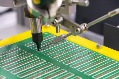
In the field of electronic manufacturing, the welding process of printed pcb directly affects product performance and reliability. As electronic products develop towards precision and multifunctionality, the limitations of traditional manual welding and fully automatic welding are becoming increasingly prominent, and semi-automatic welding technology, with its unique advantages, is becoming a key link between small-batch flexible production and large-scale efficient manufacturing.
At present, the density of semiconductor packaging continues to increase, and 0.2mm ultra-small pad welding has become a technical bottleneck in the industry. Traditional soldering iron welding is limited by manual operation accuracy, and wave soldering is prone to damage surrounding components due to excessive thermal shock. The breakthrough of laser solder ball welding technology provides a solution to this problem. Taking Dayan Zhizao's laser solder ball welding standard machine as an example, it uses a 5-megapixel CCD vision system with a sub-pixel algorithm to achieve a positioning accuracy of ±0.15mm. With a closed-loop temperature control system, the laser energy can be accurately controlled within the range of 60-150W, ensuring that the 0.2mm pad is instantly melted and the heat-affected zone is less than 0.5mm. The independently developed vacuum negative pressure solder ball conveying mechanism can stably convey 0.15-1.5mm solder balls with a ball delivery accuracy of ±0.01mm, significantly improving the welding consistency.
In the field of new energy vehicles, a company uses laser welding technology to achieve process innovation for PCB copper pillar welding. Through the 1070nm fiber laser and power closed-loop control system, the temperature control accuracy is improved to ±3℃, and the gradient coating design is combined to make the solder joint shear strength reach 45MPa. The double-station collaborative system shortens the single-point welding cycle to 3 seconds, which is 600% more efficient than traditional manual welding, perfectly solving the mass production demand of 5000+ solder joints per day.

pcb semi-automatic welding
In the field of consumer electronics, the temperature-controlled visual positioning laser soldering machine developed by Zichen Laser has been commercialized. The equipment integrates three automatic tinning methods: tin wire/tin paste/tin ball, and cooperates with the CCD visual positioning system to accurately complete the welding of QFN chips with a spacing of 0.3mm. In the production of a certain brand of TWS headphones, the equipment increased the welding yield from 89% to 99.2% and reduced the rework rate from 5% to 0.3%. The non-contact welding feature effectively avoids mechanical stress damage and is particularly suitable for precision components such as MEMS sensors.
In the field of industrial control, a company uses selective wave soldering technology to transform the production line. By programming and controlling the nozzle trajectory, multi-region differentiated welding of complex PCB boards can be achieved. In the production of inverter control boards, this technology reduces the BGA chip soldering rate from 2.1% to 0.05%, while reducing the use of flux by 60%, meeting RoHS environmental protection requirements.
China's semi-automatic PCB splitter market is showing strong growth. The market size will reach 4.5 billion yuan in 2023, and is expected to exceed 6 billion yuan in 2025, with a compound annual growth rate of 14%. Technological upgrading has become the core driving force, and the market share of laser cutting technology in semi-automatic splitters has reached 15%, an increase of 8 percentage points from 2020. The intelligent board splitter launched by a certain company integrates an AI visual inspection system, which can automatically identify the deformation of the PCB and compensate for the cutting path, so that the cutting accuracy of the special-shaped board can reach ±0.05mm.
Against the background of the accelerated transformation of intelligent manufacturing, semi-automatic welding equipment is evolving towards digitalization and networking. The digital twin welding system developed by a certain company builds a virtual model by collecting welding parameters in real time, which shortens the process debugging time by 70%. The application of 5G+ industrial Internet technology realizes remote equipment monitoring and predictive maintenance, and the OEE (overall efficiency) of a certain production line equipment has been improved to 92%.
Despite significant technological progress, the industry still faces multiple challenges. The skill gap of operators restricts the performance of equipment. A survey of a certain company shows that 73% of poor welding is caused by incorrect parameter settings. In response to this, the industry is developing an intelligent welding expert system to automatically recommend parameters through a built-in process database to lower the operating threshold. At the same time, the breakthrough of domestic core components has become the key. The laser welding head developed by a certain company has achieved a spot diameter of 30μm, breaking the foreign technology monopoly.
In terms of sustainable development, the popularization of lead-free welding technology has promoted equipment upgrades. The vacuum reflow soldering system developed by a certain company reduces the void rate of solder joints from 5% to 0.3% through a -80kPa low-pressure environment, meeting the automotive-grade reliability requirements. The popularization of nitrogen-protected welding technology has reduced the incidence of tin beads by 90%, significantly improving the welding quality.
PCB semi-automatic welding technology is reshaping the electronic manufacturing landscape with its precise, flexible and intelligent characteristics. From high-precision welding of 0.2mm tiny pads, to reliable connection of new energy vehicle power modules, to flexible production of industrial control boards, this technology continues to expand its application boundaries. With the deep integration of technologies such as AI and digital twins, semi-automatic welding equipment will evolve in a smarter and greener direction, providing key support for the high-quality development of the global electronics manufacturing industry.