What is PCB?
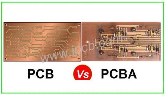
PCB is Printed Circuit Board, also known as circuit board, is an important electronic component, PCB is the supporting motherboard of the electronic component, and also the electrical connection circuit of the electronic component. Since the PCB is manufactured by printing process and subtractive etching process, it is called printed circuit board.
PCBA is (PCB + ASSEMBLY) = PCBA. Various electronic components are assembled on the PCB by surface mounting process. The next step is to assemble the box, PCB will be assembled with the outer shell to form a complete product. That is to say, the PCB before SMT is an empty PCB, there is no electronic components, such as ICs, capacitors, resistors, etc. Then through SMT and insertion, the PCB is assembled. Then through SMT and insert DIP processing, it becomes PCBA. In Europe and America, the standard writing is PCB'A, PCB and A with a dot in the middle.
What is the difference between PCB and PCBA?
PCB refers to the circuit board bare board, PCBA refers to the circuit board after processing and assembly, PCBA has been assembled with electronic components. PCBA is the finished board, PCB is the bare board.

PCB vs PCBA
PCB Design Development
1.Product demand
A programme can be in the current market to obtain a certain profit value, or enthusiasts want to complete their own DIY design, then the corresponding product demand will arise;
2.Design development
Combined with the customer's product requirements, R & D engineers will choose the corresponding chip and external circuit assembly into the PCB programme to achieve product demand, this process is relatively long, the content involved here will be described separately;
3.Sampling
R & D design of the initial PCB, procurement will be based on R & D to provide the BOM to buy the corresponding materials back to the product production debugging, trial production is divided into sampling (10pcs) the second sampling (10pcs) small trial production (50pcs ~ 100pcs) large trial production (100pcs ~ 10,000pcs) will be entered into the mass production stage.
PCB Manufacturing Process
Baking (pre-expansion)->Opening->Pre-treatment->Dry film->Exposure->Revealing->Etching->De-filming->Appearance Inspection (AOI)->Pre-treatment->Solder Resist Printing->Pre-baking->Exposure->Revealing->After baking->Printing of Character->Baking->Surface Treatment (Tin Spraying, Metallising, Gold Plating, OSP, according to the customer's needs to choose one)->Appearance Inspection->Dissection Cutting ->Appearance Inspection->Packaging->Shipping
PCBA manufacturing process of SMT SMD processing
Electronic products have to go through PCBA processing, through the PCB bare board for component mounting and insertion, then normal function test can be carried out, and then for the market. However, the manufacturing process of PCBA needs to go through one procedure after another to complete the manufacturing process.
The sequence of SMT mounting process is divided into: material baking→taking solder paste→SPI→mounting→reflow soldering→AOI→return to repair.
1.Material Baking
For wafers, PCB boards, modules and special materials that have been in stock for more than 3 months, baking at a high temperature of 120℃ for 24H should be carried out, and for MIC microphone LED lights and other objects that are not resistant to high temperature, baking at a low temperature of 60℃ for 24H should be carried out;
2. Solder Paste (Warming→Stirring→Using)
Our solder paste is stored in the environment of 2~10℃ for a long time, so it needs to be warmed up before use, and after warming up, it needs to be stirred up with a mixer before printing and use;
3.SPI3D Inspection
After the solder paste is printed on the circuit board, the PCB will reach the SPI equipment through the conveyor belt, and the SPI will inspect the thickness, width, length and the good condition of the solder surface from the solder paste printing;
4. Mounting
After the PCB flows to the laminating machine, the machine will select the suitable material to be pasted to the corresponding bit number through the set programme;
5. Reflow soldering
Paste full of material pcb flow to the front of the reflow soldering, in turn, through the 148 ℃ to 252 ℃ of the ten steps of the temperature zone, the safety of our components and PCB boards pasted together;
6.Online AOI Inspection
AOI that is, automatic optical inspection instrument, through the high-definition scanning can be just out of the furnace PCB board inspection, you can detect whether the PCB board is less material, whether the material is shifted, whether the soldering points between the tin, whether the components have a monument offset and so on;
7.Rework
For the problems found on the PCB board by AOI or manually, it needs to be reworked by the maintenance engineers, and the reworked PCB board will be sent to DIP insert together with the normal offline board.

PCBA Manufacturing
PCBA Manufacturing Process of DIP inserts
The process of DIP insert is divided into: Shaping→Installation→Wave Soldering→Cutting→Smithing→Washing→Quality Inspection.
1.Shaping
The insert materials we buy are standard materials, and the length of the pins of the materials we need is different, so we need to do the shaping of the materials in advance, so that the length and shape of the pins will be convenient for inserting or later welding;
2.insert
The arranged components are inserted according to the corresponding mould;
3. Wave soldering
The inserted board is placed on the fixture and comes to the front of wave soldering, first of all, the flux which is helpful for soldering will be sprayed at the bottom, when the board comes to the top of the soldering furnace, the tin in the furnace will float up to touch the pins, and when the tin falls down, our products will be soldered well;
4. Cutting
Due to the pre-processing of materials will have some specific requirements to leave a slightly longer pin, or the incoming material itself is not convenient for the processing of the pin, it will be manually trimmed through the pipeline to trim the pin to the appropriate height;
5. Tinning
After our PCB board through the furnace may have some pins appear hollow, pinhole, leakage of welding, false welding and other bad phenomena, our tin will be through the pipeline of manual repair to repair it well;
6. Board washing
After wave soldering, patching and other front-end links, the PCB board pin position will have some flux remains or other stolen goods attached, it is necessary for our staff to clean the surface;
7. Quality Inspection
The PCB board for the components of the error and leakage counter-check, unqualified PCB boards need to be reworked until qualified to enter the next step;
PCBA manufacturing process of PCBA test
PCBA test can be divided into ICT test, FCT test, aging test, vibration test and so on.
PCBA test is a big test, according to different products, different customer requirements, the test means are different. ICT test is the welding of components, circuit breakage detection, while the FCT test is the PCBA board input and output parameters to check whether it meets the requirements.
PCBA three anti-coating
PCBA three-proof coating process steps are: brush A surface → meter dry → brush B surface → room temperature curing →Spray thickness: spray thickness of: 0.1mm-0.3mm →All coating work should not be less than 16 ℃ and relative humidity below 75% of the conditions.
PCBA three-proof coating or a lot of, especially some of the temperature and humidity of the environment is relatively harsh, PCBA coating three-proof paint has superior insulation, moisture-proof, anti-leakage, anti-vibration, dust, corrosion, anti-aging, anti-fungi, anti-parts loosening and insulating corona and other effects can extend the storage time of the PCBA, isolation of external corrosion, pollution, and so on. Spray coating is the most commonly used coating method in the industry.
PCBA manufacturing process of finished product assembly
The PCBA board will be coated and tested OK for the assembly of the shell, and then carry out the whole machine aging and testing,through the aging test no problem products can be shipped.
From PCB design, PCB manufacturing to PCBA manufacturing is a ring with a ring, PCBA manufacturing process in any one of the links in the problem will have a very big impact on the overall quality, the need for each PCBA manufacturing process to carry out strict control.