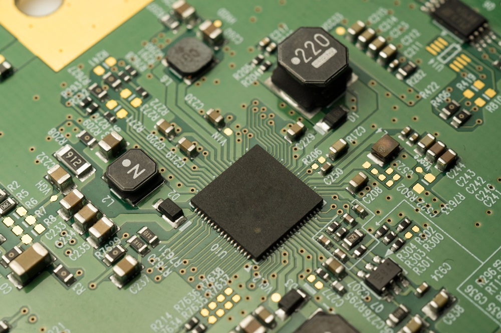
PCBA (Printed Circuit Board Assembly) and PCB (Printed Circuit Board) mainly have the following differences:
First, the concept of definition.
PCB refers to the printed circuit board, which is a printed etching and other processes in the insulating material (such as fiberglass, epoxy resin, etc.) on the substrate to form a conductive line and graphic carrier of electronic components. Its main function is to provide physical support and electrical connections for electronic components. For example, our common computer motherboard part of the substrate, before the installation of the CPU, memory and other components, is a PCB.
PCBA is a printed circuit board assembly, is based on the PCB, through the surface mount technology (SMT), plug-in technology, etc. will be a variety of electronic components (such as chips, resistors, capacitors, inductors, etc.) mounted and welded to the PCB, forming an electronic component with a complete function. For example, the motherboard of a cell phone that has been installed with all components and tested to work properly is PCBA.
Second, the composition of the structure.
PCB
Mainly by the substrate, conductive lines (copper foil), through-hole, pads and other components.
Substrate is the basic material of the PCB, providing mechanical support and electrical insulation. Common substrate materials are FR-4 (epoxy glass fiber cloth board), which has good mechanical properties, electrical properties and chemical stability.
Conductive lines are used to connect the pins of various electronic components for signal transmission and power distribution. Vias are used to connect the conductive lines between the different layers to enable signal transmission in multi-layer PCBs. Solder pads are metal areas used for soldering the pins of electronic components. Their size, shape and spacing are designed according to the type of package and electrical requirements of the components.
PCBA
In addition to all the components of a PCB, PCBA includes a variety of electronic components and soldering materials.
There are a wide variety of electronic components, which can be divided into active devices (such as integrated circuit chips, transistors, etc., which can amplify electrical signals, switching, etc.) and passive devices (such as resistors, capacitors, inductors, etc., which are mainly used to regulate the parameters such as current, voltage, frequency, etc.) according to their functions. These components are fixed on the pads of the PCB by soldering, and the soldering materials (such as solder paste, solder wire, etc.) form solder joints during the soldering process to ensure the electrical and mechanical connection between the components and the PCB.

PCBA
Third, the production process.
PCB production process
Mainly includes design, plate making, etching, drilling, surface treatment and so on.
The design stage is based on the circuit function and performance requirements, the use of professional electronic design automation (EDA) software to design the PCB layout, to determine the layout of the line, component packaging, hole location. Plate making is to convert the designed layout data into production light drawing files, and then through photolithography technology to transfer the graphics to the copper-clad board. The etching process utilizes chemical etching to remove unwanted copper foil to form conductive lines. Drilling is used to create vias and mounting holes for components. Surface treatment (e.g. tin spraying, gold immersion, etc.) is used to improve the solderability and corrosion resistance of the pads.
PCBA production process
PCBA production process includes component procurement, component testing, mounting, insertion, soldering, cleaning, testing and so on.
First of all, we have to purchase qualified electronic components according to the BOM (Bill of Materials), and test the components to ensure that their parameters and quality meet the requirements. SMD process is through the automatic placement machine will surface mount components (SMD) accurately mounted to the PCB's designated pads, and then reflow soldering, so that the components and the PCB to form an electrical connection. Plug-in process is not the use of surface mount components (such as some power devices, connectors, etc.) into the corresponding holes in the PCB, and then wave soldering or manual welding. After the completion of welding, cleaning is required to remove the welding process residual flux and other impurities. Finally, functional tests, electrical performance tests and other tests are conducted to ensure that the PCBA meets the design requirements.
Fourth, the functional use.
PCB
Individual PCB itself does not have a complete electronic function, it is mainly as a basic platform for the installation of electronic components and circuit connections to provide physical support and electrical pathways. For example, an empty PCB can be regarded as the “skeleton” of an electronic device, waiting for the installation of components to give it function.
PCBA
A PCBA is a complete electronic assembly capable of performing a specific electronic function. For example, in a communication device, PCBA can complete the signal modulation, demodulation, amplification, filtering and other functions; in a control device, PCBA can realize the control of external devices, data acquisition and processing and other functions.