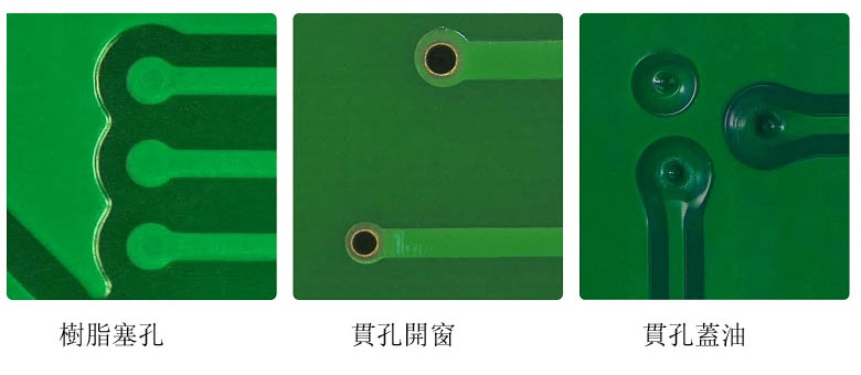
What is plated hole filling? What is Resin Plugging?
Resin hole plugging is the use of solvent-free ink to plug holes, in addition to complementing the general ink is not easy to fill the problem, but also to reduce the ink heat generated by ‘cracks’, usually for the vertical and horizontal larger through-hole diameter when used.
Electroplating hole filling now is to use the characteristics of additives to control the growth rate of each part of the copper to fill the holes, mainly used in continuous multi-layer superposition of holes (blind hole process) or high current design.

PCB Plug Hole
PCB hole plugging is usually used to fill the heat sink (Termal Pad) with a hole diameter of 0.55mm or less by applying a second layer of ink (green paint) after the anti-solder layer. The purpose of hole plugging in the PCB manufacturing process is to avoid short-circuiting caused by tin penetration during the tinning process when DIPs are loaded on the components, especially in BGA design. PCB hole plugging can maintain the surface flatness and meet the customer's requirements for characteristic impedance to avoid damage to the circuit signals.
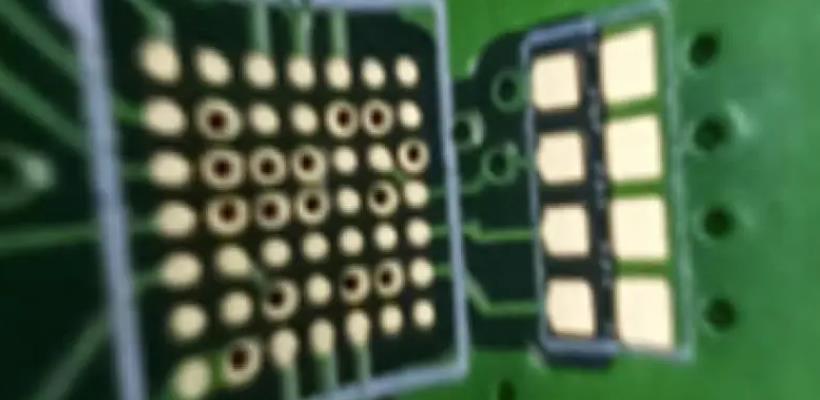
The process of using resin to plug holes in PCBs is often used for BGA parts because traditional BGAs may be used to make a via in pad to the backside, but if the BGA is too dense to make the via go out, it is possible to drill holes directly from the PAD and make a via in pad to the other layer, and then fill the holes with resin to make the via in pad with copper plating, which is commonly known as the VIP process. This is commonly known as the VIP process (via in pad). If the via in pad is done without plugging the holes with resin, it is easy for tin to leak out and cause short circuits on the back side as well as solder gaps on the front side.
The general PCB resin plugging process includes drilling, plating, plugging, baking, and grinding. After drilling, the holes are plated through, then plugged with resin and baked, and then ground to a smooth finish, and after the resin is ground, because it does not contain any copper, it is necessary to add another layer of copper to turn it into a PAD. This process is done before the original PCB drilling process, i.e., the holes to be plugged are processed first, and then the other holes are drilled according to the original normal process.
If the holes are not plugged properly and there are bubbles inside the holes, the boards may explode when they go through the tin oven because the bubbles absorb moisture easily. However, if there are bubbles inside the holes in the process of plugging the holes, the bubbles will squeeze out the resin during the baking process, resulting in the situation where one side of the board is depressed and the other side of the board is protruding, and the defects can be detected at this time. Therefore, if the freshly baked boards or sub-packages are baked during assembly, then the⾔ will not cause the PCBs to explode.

PCB Through Hole
What is the difference between plated and resin plugged holes?
1.The surface of plated and resin plugged holes are different.
Plating hole filling is to fill up the hole by copper plating, the surface of the hole is full of metal,while resin plugging is to fill up the epoxy resin by copper plating on the wall of the hole, and then copper plating on the surface of the resin, the effect is that the hole can pass through, and there is no indentation on the surface,which doesn't affect the soldering.
2.Different processing procedures for plating hole filling and resin hole plugging
Electroplating hole filling is through the plating will be directly filled with holes,no gaps,the benefits of welding,but the process requires high capacity,the general PCB manufacturers can not do.Resin plug holes is the hole wall after plating copper, filled with epoxy resin to fill the holes,and finally plated copper on the surface,the effect is similar to no holes,good for welding.
3.The price difference between plated hole filling and resin hole plugging
Plating hole filling has good oxidation resistance, but the technology requirement is high and the price is expensive.Resin plug holes have good insulation and are cheaper.
Before plating hole filling and resin hole plugging technology is not popular,PCB manufacturers generally use a relatively simple process of green oil hole plugging technology, but the green oil hole plugging will shrink after curing, easy to air blowing problems, can not meet the user's high saturation requirements. Electroplating hole filling and resin plugging process plugs the buried holes of the inner HDI layer before pressing, which perfectly solves the drawbacks of green oil plugging and balances the conflict between the control of dielectric layer thickness of pressing and the design of the buried holes of the inner HDI layer.
Although plating and resin plugging processes are relatively complex and costly, but the saturation. The quality of plated and resin plugged holes is more advantageous than that of green oil plugged holes.