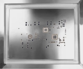
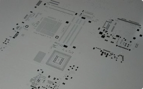
In the process of PCB (printed circuit board) manufacturing and SMT (surface mount technology) assembly, stencil with frame and stencil without frame are key process tools, and they are often confused because of their similar names. However, there are essential differences between the two in terms of functional positioning, structural design, manufacturing process and application scenarios.
1. Functional positioning
The core function of stencil with frame is solder paste printing control. As the first process of SMT assembly, the steel mesh forms holes corresponding to the PCB pads on the stainless steel sheet through laser cutting or electroforming process, and its function is similar to a "precision screen". During the printing process, the stencil with frame fits the PCB surface, and the scraper evenly coats the solder paste on the pad through the holes to ensure that the amount of tin in each solder joint is accurately controlled. For example, in the 0201 chip package, the aperture of the stencil with frame must be accurate to 0.3mm, and the roughness of the hole wall must be ≤3μm to avoid the risk of short circuit caused by solder paste residue.
Stencil without frame mainly undertakes positioning and support functions. In precision manual screen printing stations or small PCB assembly, steel sheets are often used as auxiliary tools:
Positioning function: Fix the PCB position by adjusting the pillars on the Z axis to ensure that the steel mesh and the PCB pad fit tightly. For example, a certain model of precision screen printing station adjusts the height of the positioning pillars through the bottom screws to control the fitting error between the steel sheet and the PCB within ±0.05mm.
Support function: In flexible PCB (FPC) assembly, steel sheets can be used as rigid backplanes to prevent PCB deformation during printing. A mobile phone FPC manufacturer uses 0.2mm thick stainless steel sheets as support to reduce the printing offset rate from 3% to 0.5%.

stencil
2. Structural design
The steel mesh is a full-board covering structure, and its size is exactly the same as the PCB board surface, and the thickness is usually between 0.1-0.3mm. According to process requirements, stencils can be divided into three categories:
Solder paste stencil: The holes directly correspond to the pads and are used for reflow soldering. A high-end server PCB uses a stepped stencil, which is locally thinned by 0.05mm in the BGA area to control the amount of tin in large-size solder balls.
Red glue stencil: The hole is located in the middle of the component pad and is used for glue fixation before wave soldering. An industrial control board reduces the component displacement rate from 15% to less than 2% through the red glue steel mesh.
Dual process stencil: Combines solder paste and red glue functions, suitable for mixed assembly processes. An automotive electronics manufacturer uses a double-layer steel mesh structure, with solder paste printed on the upper layer and red glue applied on the lower layer, to achieve full board assembly in a single furnace.
Stencil without frame is mostly small-sized sheets for local application, with common specifications ranging from 50mm×50mm to 200mm×200mm. Its design features include:
Edge treatment: Chamfering or polishing process is used to avoid scratches during manual operation. A laboratory test showed that unchamfered steel sheets caused 30% of operators to cut their hands when wiping and cleaning, while the risk was reduced to zero after chamfering.
Thickness customization: Adjust the thickness according to the support requirements. The thickness of the flexible PCB support steel sheet is usually 0.1-0.5mm, while the high-precision positioning steel sheet can reach 1.0mm.

stencil without frame
3. Manufacturing process
Steel mesh manufacturing belongs to the field of ultra-precision processing, and the core processes include:
Laser cutting: Using fiber laser to cut holes on 304 stainless steel sheets, the accuracy can reach ±0.02mm, but the hole wall is prone to slag. A manufacturer reduced the roughness of the hole wall from 8μm to 3μm through electrolytic polishing technology, which increased the solder paste release rate by 12%.
Electroforming: The hole wall is formed by electroplating nickel layer, which is suitable for ultra-fine pitch components below 0.3mm. A semiconductor packaging company uses electroformed steel mesh to reduce the empty soldering rate of QFN devices from 5% to 0.3%.
Hybrid process: Combining laser cutting and chemical etching to achieve different thicknesses in local areas of the steel mesh. A mining machine PCB manufacturer uses a hybrid process steel mesh to increase the amount of tin in the heat dissipation pad in the high-power chip area by 30%.
Steel sheet manufacturing focuses on the balance between cost and efficiency, and the main processes include:
Stamping: Using a mold to punch out positioning holes or support structures, the cost is 60% lower than laser cutting, but the accuracy can only reach ±0.1mm.
CNC machining: CNC milling machines are used to process complex contours, which is suitable for special-shaped PCB support. A medical equipment manufacturer uses CNC steel sheets to control the printing deviation rate of circular FPC within 0.1mm.
Surface treatment: Sandblasting or anodizing processes are used to improve wear resistance. A consumer electronics manufacturer uses hard anodizing to increase the service life of steel sheets from 500 times to 2000 printing cycles.
4. Industry application
Steel mesh is a core consumable in high-end electronic manufacturing, and its application scenarios include:
Server and data center: A cloud computing manufacturer uses 0.08mm thick electroformed steel mesh to increase the BGA welding yield of Xeon processor PCB to 99.95%.
Automotive electronics: A new energy vehicle company uses steel mesh aperture compensation technology to reduce the welding void rate of IGBT modules from 8% to below 1%.
Aerospace: A satellite PCB manufacturer uses titanium alloy steel mesh to maintain dimensional stability in the -55℃ to 125℃ temperature cycle test to ensure the reliability of solder joints.
Steel sheets are widely used in small and medium batches and prototype manufacturing:
R&D laboratory: A university laboratory uses an adjustable steel sheet bracket to simulate PCB thickness by replacing steel sheets of different thicknesses, shortening the new product development cycle by 40%.
Flexible electronics: A wearable device manufacturer uses 0.1mm thick steel sheets to support FPC, increasing the printing pass rate of 0.3mm pitch components from 70% to 95%.
Maintenance market: A third-party maintenance company has developed a modular steel sheet library that covers 90% of mainstream mobile phone models, reducing the BGA rework time from 2 hours to 30 minutes.
The difference between stencil with frame and stencil without frame is essentially the balance between precision manufacturing and flexible production. Stencil with frame achieves large-scale industrial production through micron-level precision control, while stencil without frame meets diverse customization needs with millimeter-level tolerance.