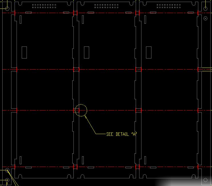
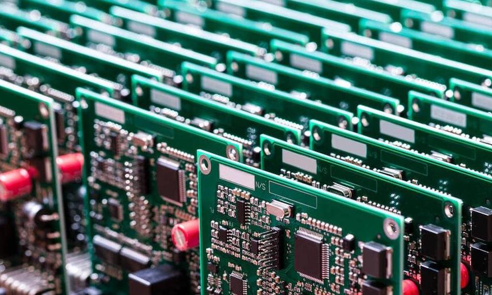
Now I would like to share with you the impact of PCB on SMT. PCB is a technology and an art. PCB board connection is a direct way to put several small PCB units together with various kinds of connecting channels. Comparison of common board with AA sequential spelling, AB positive and negative spelling, AA rotating spelling, AB yin and Yang spelling, ABC mixed spelling and so on many ways.
PCB design engineers will usually take into account the product structure size, electrical performance, component layout and other functional aspects. How to enhance the SMT production efficiency in the design of the board, to minimise the risk of impact on product quality, PCB form factor is not regular, after the impact of the board production efficiency,while it also adds production difficulties and SMT manufacturing costs.
The purpose of the PCB board:
1.Because the PCB form factor is too small and irregular,it seriously affects the SMT production efficiency.
2.Maximise the utilisation rate of the board and reduce the cost.
3.Reduce production difficulty and improve product yield.

PCB boards
PCB design rules:
There are many kinds of PCB design pipeline,in the new product trial stage sometimes it is difficult to determine which pipeline, the number of connected boards is optimised. PCB design engineers according to product characteristics (such as product structure limit, external interface limit height,limit bit and other factors) in the design priority to meet the structural requirements of the product, followed by the PCB board and SMT processing process to respond to the PCB board utilisation and production efficiency issues raised.In the production process after the selection of PCB boards, encountered different geometric dimensions and thermal expansion of the PCB connecting pipe after the furnace directly affects the reliability and performance of the product,adding to the SMT production processing difficulties and manufacturing costs.
Combined with years of experience of SMT process engineers, the use of PCB piping to enhance the efficiency of SMT production lines.
In the SMT foundry line in order to enhance the production line crop rate, the common connecting pipeline has AAAA splicing or AB splicing two major pipelines, we can not directly ask which one connecting pipeline is good? This should be considered from the complexity of the product process, the balance rate of the production line machine mounting cycle after connecting the board, the large size of the components of the second remelting after the problem of dropping pieces and so on.
1.The advantages of adopting the forward and backward collocation design (AABB collocation) is to make the SMT production line equipment configuration and process flow simple and easy. A steel mesh, a set of SMD programme and SPI / AOI inspection programme and reflow soldering furnace temperature curve optimization once, etc., to enhance the SMT fast line speed and the first piece of verification is completed once in a very short period of time PCBA finished products are produced to the next process function test.
2.The disadvantage of adopting the positive and negative spelling design (AABB spelling) is that, if the product BOT surface and TOP surface in the layout of the components in the case of large differences (the main wafer volume is larger, higher density of component layout, through-hole reflow component feet beyond the board, etc.) will result in small spacing position of the solder paste printing is poor and unstable, the volume and weight of the components of the second over the furnace risk of dropping the pieces in mass production not only does not solve the problem of efficiency improvement will also bring processing difficulties. In mass production, not only does it not solve the problem of efficiency improvement, but also brings processing difficulties and quality problems, which is also a test of the engineer's ability to tackle online technology.
3.Using (AAA / BBB spell) non-positive and negative spell design,more suitable for the majority of factories now recommended, the production line is easy to deploy and rational arrangement of equipment resources, production process stability, it is easy to enhance the efficiency of the production line.In the PCB design engineers must consider the overall main chip components, heat dissipation components, and external interface components layout reasonableness, the processing plant only need to reasonably arrange the production line Mr. production BOT surface (less components surface) regeneration of the production TOP surface (multi-component surface), the processing process encountered quality anomalies in the process of process engineering is easier to deal with the solution.
In the SMT foundry process, under the premise of guaranteeing the straight-through rate, what kind of connecting pipeline is the best? According to the SMT machine put aside and equipment processing capacity, process stability and other factors to consider.

PCBA
iPCB is a very important part of the PCB connection in order to satisfy the high efficiency of the output of the laminating machine every hour:
1.Any side of the single board size less than 80mm need to be connected to the board design.
2.The maximum size of the PCB after connecting the board (L) 300-350mm * (W) 200-250mm is more appropriate.
3.Multi-connected boards between the profile of the board edge connector beyond the profile of the interference, through the rotary splicing + process edge pipeline solution to prevent damage to the quality of the welding process in the transmission or transport of collision pieces of poor quality.
4.Some irregular shape of the PCB skeleton area is larger, in SMT production is likely to lead to equipment transfer track PCB sensor misrecognition, resulting in incorrect action or failure to sense the PCB appeared on the stacked board phenomenon, in the design of the board with the addition of new technology edge to make up for the skeleton position.
5.After the design of the board must ensure that the edge of the reference point of the board away from the board edge to less than 3.5mm (machine in the clamping PCB board edge of the minimum range of 3.5mm), the board on the two diagonal reference point can not be placed symmetrically, front and back of the reference point should not be placed symmetrically, so that the equipment's own identification function to prevent daze PCB reverse/reverse side into the machine.
6.Connected to the board design process, the number of connection points between the single board and the placement of the location is also very important.
7.For the FPC and rigid-flexible bonded board with the board pipeline is very different, the requirements of the board will be more consideration.
8.PCB board design to meet the PCB board utilisation and production processing efficiency issues, but also to consider the production of PCBA thermal deformation after the furnace and sub-panel efficiency issues.