In the semiconductor industry chain, packaging and testing are the key links connecting chip design and terminal applications, and wire bonding equipment, as the core tool of the packaging link, undertakes the important task of realizing the electrical connection between the chip and the external circuit. With the rapid development of technologies such as 5G, artificial intelligence, and the Internet of Things, the technical iteration and application scenario expansion of wire bonding equipment are profoundly affecting the future pattern of the semiconductor industry.
1. What is wire bonding equipment?
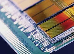
Wire bonding is a process of connecting the chip pad to the package substrate or pin through extremely fine metal wires (such as gold wires, copper wires, and aluminum wires). Its core equipment consists of modules such as precision motion platforms, bonding heads, visual systems, and ultrasonic generators. The melting bonding of metal wires is achieved through hot pressing, ultrasonic or thermal ultrasonic composite energy. This process must be completed at micron-level precision to ensure the mechanical strength and electrical performance of the bonding point.
Technical advantages:
High reliability: The bonding point can withstand environmental stresses such as thermal cycling and mechanical vibration to ensure the long-term stability of the device.
Flexibility: Supports a variety of packaging forms (such as QFP, BGA, SIP), adapting to the diverse needs from consumer electronics to automotive electronics.
Cost-effectiveness: Compared with advanced packaging technologies such as flip chips, wire bonding has a mature process and low equipment investment, and is still the preferred solution for the mid- and low-end markets.
2. Technological evolution: A leap from traditional to intelligent
Material innovation:
In the early days, gold wire was the main method, but copper wire gradually became the mainstream due to its cost advantage (the price is only 1/3 of that of gold wire) and improved conductivity. Copper wire bonding needs to overcome the oxidation problem, and equipment manufacturers have broken through bottlenecks by optimizing bonding parameters and introducing inert gas protection.
Precision breakthrough:
As the chip feature size decreases, the bonding pitch moves from 100μm to less than 30μm. The equipment needs to be equipped with high-speed and high-precision motion control systems (such as linear motors, air bearings) and sub-micron visual positioning technology.
Automation and intelligence:
AI empowerment: Optimize bonding parameters through machine learning, monitor bonding quality in real time, and reduce manual intervention.
Flexible manufacturing: Modular design supports fast line change and adapts to the needs of multi-variety and small-batch production.
Digital twin: Virtual simulation bonding process, shortening process development cycle.

wire bonding
3. Application fields and market structure
Consumer electronics: In smartphones and wearable devices, wire bonding equipment is used to encapsulate power management chips, sensors and other devices, supporting the trend of thin and light design.
Automotive electronics: In the packaging of vehicle-mounted MCUs and power modules, it is necessary to meet harsh environmental requirements such as high temperature, high humidity, and high vibration, and promote the development of equipment towards high reliability.
Industrial and medical: Industrial controllers and implantable medical devices have extremely high requirements for long-term packaging stability. Wire bonding technology continues to expand its boundaries through material improvements (such as silver alloy wires) and process optimization (such as wedge bonding).
Global market:
Asian manufacturers (such as K&S and ASM Pacific) dominate, and European and American companies (such as Kulicke & Soffa) remain competitive in the high-end market.
Chinese local equipment manufacturers (such as China Electronics Technology Group Corporation 45th Institute and Han's Laser) accelerate domestic substitution and achieve breakthroughs in discrete devices and LED packaging.
4. Technical Challenges and Future Trends
Miniaturization Limits:
When the bonding pitch approaches 10μm, physical limitations such as material deformation and capillary effect become prominent, and new bonding technologies (such as laser-assisted bonding) need to be explored.
Heterogeneous Integration Demand:
With the rise of chiplets and 2.5D/3D packaging, wire bonding needs to be integrated with micro-bumps, TSV and other technologies, and equipment needs to have multi-process compatibility.
Green Manufacturing:
Reduce the use of precious metals such as gold and silver, develop environmentally friendly bonding materials (such as palladium-plated copper wire), and optimize energy consumption management.
Wire bonding equipment is the core engine and technological evolution of semiconductor packaging, and its technological progress is directly related to the performance boundaries and cost structure of electronic products. In the future, with the penetration of advanced packaging technology and the deepening of intelligent manufacturing, wire bonding equipment will continue to make breakthroughs in precision, efficiency, and intelligence, injecting inexhaustible power into innovation in the semiconductor industry.