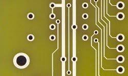
In the world of printed circuit board (PCB) manufacturing, solder mask is often considered a default feature. It offers protection, enhances aesthetics, and aids in automated soldering. However, in specific technical scenarios, PCBs without solder mask—often called "bare copper boards"—are not only acceptable but actually preferable. In this article, we take a deep dive into the rationale, use cases, and technical considerations behind choosing PCBs without solder mask.
1. What Is a PCB Without Solder Mask?
A PCB without solder mask is simply a circuit board where the copper traces are exposed without any overlay of the typical green (or other colored) polymer coating. The solder mask usually acts as an insulating and protective layer. Without it, all the copper circuitry remains visible and unprotected.
2. Key Scenarios Where Solder Mask Is Removed or Omitted
a. High-Frequency and RF Applications
In high-frequency RF or microwave PCBs, solder mask can influence signal performance. The dielectric constant (Dk) of solder mask is typically higher than air and may introduce impedance variation or signal loss, especially in tightly controlled stripline or microstrip layouts. Engineers working with PTFE-based laminates or ceramic-filled substrates often exclude solder mask to maintain impedance control.
b. Edge Plating and Castellation Requirements
When a board involves edge plating or castellated holes (common in RF modules or board-to-board connection modules), the plating process often requires the copper at the edge to be completely exposed. Applying solder mask in these areas would interfere with plating continuity and surface finish.
c. Wire Bonding
In microelectronics or semiconductor packaging applications, gold wire bonding is often used. Solder mask interferes with the bonding process, so these areas must be kept free of any polymer coating. ENIG (Electroless Nickel Immersion Gold) finishes are usually applied directly on exposed copper pads.
d. Selective Soldering or Hot Bar Soldering
Some specialized soldering processes like hot bar reflow or selective soldering require completely exposed copper pads for uniform heat transfer. Solder mask may act as a thermal insulator and disrupt this process.
e. Cost-Driven Prototyping or Quick Turn Projects
In early-stage prototyping or internal testing, engineers sometimes opt for no solder mask to reduce fabrication turnaround time or cost. Many low-volume, quick-turn PCB houses offer bare copper options that allow engineers to iterate quickly.
3. Material and Surface Finish Considerations
Choosing to go without solder mask has downstream implications, particularly in terms of surface finish and oxidation prevention:
Surface Finish: Because the copper is exposed, it must be protected via surface treatments. Common finishes for bare boards include ENIG, immersion silver, OSP (Organic Solderability Preservative), or hard gold. These prevent oxidation and maintain solderability.
Oxidation Risk: Bare copper oxidizes quickly, which can severely affect solderability and long-term reliability. Hence, choosing an appropriate finish is even more critical when solder mask is absent.
Material Compatibility: High-frequency laminates such as Rogers, Taconic, or Arlon may behave differently when not covered by solder mask. Engineers should verify thermal and mechanical behavior in accelerated life tests.

4. Design and Manufacturing Challenges
a. Solder Bridging Risk
One of the main functions of solder mask is to prevent solder bridges during reflow. Without it, designers must ensure sufficient pad spacing and careful stencil design to avoid unintended shorts.
b. Contamination and Handling
Exposed copper is vulnerable to contamination from oils, fingerprints, and dust. Manufacturing must be done in clean environments with strict ESD and handling protocols.
c. Visual Inspection Complexity
Lack of color contrast can make AOI (Automated Optical Inspection) and manual inspection more difficult. Inspectors rely on the color differentiation between pads and mask to identify defects quickly.
5. When Is It a Bad Idea?
While solder-mask-less designs serve a purpose, there are many cases where omitting solder mask is a poor decision:
Mass production with fine-pitch components
Consumer electronics requiring environmental protection
Boards with high density interconnects (HDI)
In such cases, the reliability, manufacturability, and inspection benefits of solder mask outweigh its disadvantages.
6. Tips for Engineers Specifying PCBs Without Solder Mask
Always specify the exact finish (e.g., ENIG, OSP) when solder mask is omitted.
Include a note in the fabrication drawing explaining the reason for omitting solder mask.
Work closely with your PCB fabricator to ensure that handling and surface protection protocols are in place.
Use generous spacing in pad design to reduce the risk of bridging.
Avoid BGA and fine-pitch components unless absolutely necessary.
Conclusion
PCBs without solder mask are not a mistake—they are a deliberate engineering choice in specific technical contexts. Whether for signal integrity, manufacturing constraints, or prototyping speed, going maskless can be the right call when designed and executed properly. Understanding the trade-offs and communicating clearly with your fabricator are key to making this choice work for your design.