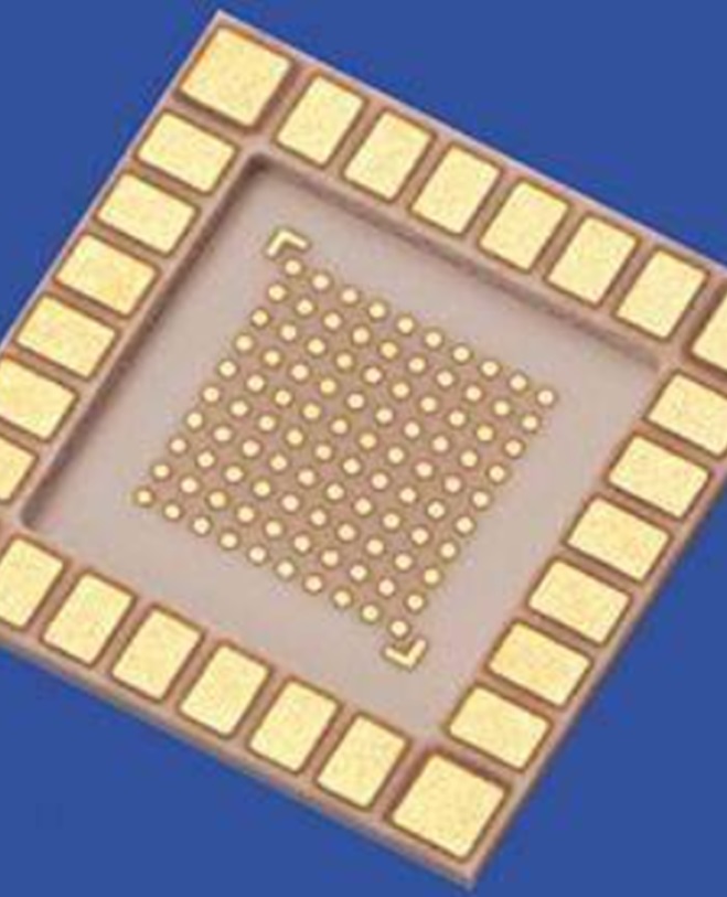
As we all know, there are three technologies in total to manufacture multilayer ceramic circuit boards, they are thick film ceramic PCB, HTCC ceramic PCB and the last one is LTCC ceramic PCB. LTCC ceramic board was developed from HTCC technology in the early 1980s. With the rapid development of electronic products, LTCC PCBs have become popular in recent years due to its unique advantages over traditional PCBs. They are highly reliable, durable, have excellent electrical and mechanical properties, and are very suitable for high-performance electronic applications.
Unlike HTCC ceramic boards, the sintering temperature of LTCC is around 950oC (900-1000oC), at which temperature, the ceramic substrate is easily combined with the copper layer to form a non-interference high-density circuit in three-dimensional space, and to some extent, it can also be made into a 3D substrate with passive components. LTCC PCB is made of ceramic substrate/glass material as dielectric layer, high conductive metal materials such as gold, silver, alloy (such as Pd/Ag, Pt/Ag) as electrode layer, parallel printed circuits, and then sintered at 1000oC. Currently, ceramic multilayer PCBs are used most in high-speed, high-power circuit applications. These boards have been shown to reduce parasitic capacitance by up to 90% compared to traditional circuit board materials, and have broad prospects for future applications in aerospace, medical equipment, industrial and automotive industries.

LTCC technology involves stacking and laminating multiple layers of ceramic green tape, which are then co-fired (sintered) at relatively low temperatures (usually between 850°C and 950°C) to form a monolithic structure. Each layer can be patterned with conductive materials such as tungsten or gold to form a dense multilayer circuit board with embedded passive components and sealed packaging. One of the biggest features of LTCC technology is that it realizes the possibility of using different layers to make 3D structures. With the development of technology, the requirements for the performance and function of electronic components and assemblies are getting higher and higher, while the size of the product is required to be smaller and smaller. LTCC technology can meet these two requirements, so it has been widely used in the field of microelectronics. LTCC technology is the mainstream technology for passive integration. LTCC can realize the packaging of three basic components (resistors, capacitors, inductors) and various passive components (such as filters, transformers, etc.) in a multi-layer wiring substrate, and integrate them with active components (such as power MOS, transistors, IC modules, etc.) into a complete circuit system. For a long time, PCB boards have been used in circuits to achieve electrical interconnection. However, since passive components based on ceramic materials such as resistors, capacitors, inductors, and filters require high-temperature sintering, they cannot be integrated in multi-layer PCB boards, and the necessity of LTCC technology is apparent.
The main advantages of LTCC PCBs include:
High-frequency performance (up to millimeter wave frequencies).
Low dielectric loss and low signal propagation delay.
Excellent thermal conductivity and stability.
Good sealing and resistance to harsh environments.
Integration of passive components (resistors, capacitors, inductors).
High reliability and long service life.
These unique characteristics make LTCC PCBs very suitable for a wide range of applications, including:
Aerospace and defense systems.
Automotive electronics.
Telecommunications.
Medical equipment.
Industrial sensors and controllers.
What materials are commonly used in LTCC PCBs?
The most commonly used ceramic materials for LTCC PCBs are alumina (Al2O3) and glass-ceramic composites. Conductive materials such as tungsten, gold, and silver are used to pattern conductive traces and vias.
Can LTCC PCBs be repaired or reworked?
Due to their monolithic structure and co-fired manufacturing process, LTCC PCBs are generally difficult to repair or rework. Any modification or repair requires specialized techniques and equipment, making it difficult and costly.
Each type of ceramic PCB has its own unique advantages and disadvantages, and the choice of PCB type depends on the specific requirements of the application. LTCC ceramic PCBs are the mainstream for passive integrated circuits and a popular choice for high-frequency/high-speed applications.