PCB designers in the design of the circuit board,often reserved for the edge of the board. Do you know the reason for doing so? What are the advantages of designing pcb with board edges?
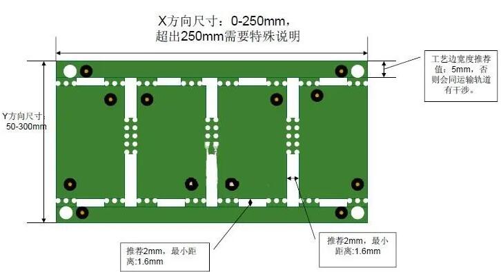
Although the edge of the board is not a real element of the PCB circuit board,but for the PCB assembled by surface mount technology, it plays a very important role. The PCB edge, also known as the working edge, is a long strip of blank board edges that are set up to allow for track transfer locations and placement of marking points during SMT processing. PCB is ultimately to be SMT SMD processing, PCB in the SMT production line is transmitted through the rail, this, must leave a pair of forbidden components of the edge as a transmission edge. Usually the two long edges of the PCB or the large board after the board as its transmission edge.
In the PCB circuit board production process,with the board edge of the reservation for the subsequent SMT patch processing has a very important significance.The board edge is a new part added on two or four sides of the PCB in order to assist SMT mounting,DIP insertion and soldering board.
Because the track of the SMT mounting machine is used to clamp the PCB and flow through the mounting machine,the electronic components too close to the edge of the track are prone to collision when they are sucked up by the suction nozzle of the SMT mounting machine and mounted on the PCB board,which can't complete the production.
This must reserve a certain amount of board edge,can be a good solution to these problems encountered by the PCB circuit board in the SMT patch.Similarly,the reserved edge is also suitable for some inserted components to prevent the similar phenomenon when passing through wave soldering.

Design PCB with board edges
PCB edge can effectively control the size and shape of the board.By controlling the width and shape of the PCB edge during PCB processing,it can ensure that the dimensions of the board are consistent with the design requirements. This is critical to the proper functioning of the electronic equipment,because if the board size does not meet the requirements,it may result in the electronic components can not be installed correctly,thus affecting the function of the entire equipment.
The PCB edge also serves to protect the circuit board.With additional processing,the edge of the board prevents the board's edges from being exposed to the outside environment,thus reducing the risk of damage due to the effects of the outside environment.Electronic equipment is usually used in various harsh conditions,such as high temperature and humidity,etc.If the circuit board is not properly connected to the edge of the board,it may be attacked by these factors, resulting in a decline in the overall performance of the equipment or failure.
PCB edge can also improve the strength and stability of the board.The edge adds mechanical strength to the board,making it more resistant to external shocks and vibrations.In addition,edgebanding reduces board deformation and warpage, ensures the stability and reliability of electronic components,and extends the life of equipment.
What should be considered on the board edge?
1.The width of the board edge. Generally speaking, the width of the edge of the board is within the range of 1.5mm to 5mm according to the specific assembly requirements and parameters of the assembly equipment.In this case,it is very important to consult the contract assembler to ensure that your design is compatible with the corresponding assembly equipment.
2.Cost of the edge.With the manufacturing of PCBs,data consumption will definitely increase, and so will the total cost of comics.How to balance the PCB cost and manufacturability can be regarded as the primary consideration of PCB design engineers and PCB manufacturers or assemblers.To minimise cost,the usual approach is to minimise the application of board edges by designing the optimum layout for the PCB panel, which minimises the application of board edges. A reliable PCB manufacturer or assembler has the knowledge and experience to provide the customer with the ideal solution based on quality and cost considerations.

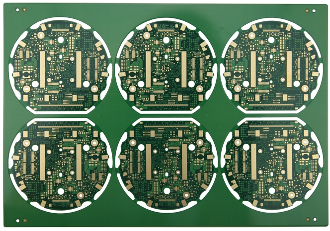
PCB with board
How to separate the board edge?
The edge of the board is not part of the PCB and can be removed after the PCBA processing is completed. The method of removing the edge of the PCBA board can be roughly divided into three categories: V-cut separator, milling separator and manual de-emphasis.
1.Splitting machine. For quality alone,it is the most effective choice.The machine mainly relies on the milling cutter, the milling cutter can be programmed according to the route of the panel PCBA high-speed rotary separation into separate parts. It has a distinct advantage over V-cut board machines,which can only cut panels along straight lines, and far beyond. In addition, this results in clean and tidy panel edges, whereas V-cut strippers or manual strippers usually result in blurring. As such,it helps to improve quality and reduce waste,but is expensive due to the complexity and low flexibility of the process.
2.V-Cut Slitting.It can be cut along the V-groove in a straight line pipe and the cost of blade consumables is higher. However, the total cost is lower than that of the board splitter.
3.Manual Depaneling.It relies on hand or sharp-nosed pliers for separation,with the advantages of easy operation and low cost. However, it may generate greater mechanical stress, so that the board edges near the components may be struck through.
The above is to share why to design PCB with board edge, with board edge can be a good solution to the PCB in the SMT paste the problems encountered.