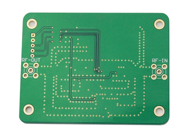
PCB soldermask is an essential material for printed circuit boards. Soldermask protects the board from oxidation, corrosion, and contamination, while soldermask can also play a role in reinforcing the board's surface hardness, facilitating soldering, and enhancing the board's aesthetic appearance. As an insulating layer, the soldermask protects exposed copper areas from environmental factors such as moisture and dust that can cause oxidation and corrosion over time. Additionally, the soldermask layer helps identify the area where solder should be applied, resulting in more accurate and reliable solder joints during assembly.
Soldermask Printing Methods: There are two types of printing: manual printing and machine printing. The most conventional is machine printing, but for small batch production using manual printing is also feasible.
Soldermask ink thickness: generally between 25-30um. Too thick to cause bubbles, and short circuits, too thin to provide effective protection. General solder resists on the printed circuit board thickness of 0.02-0.05mm.

Soldermask ink hardening time: different models of ink hardness vary, low hardness, generally only 5-10 minutes, while the higher hardness, it may take 30-60 minutes. If the hardening time is too short or too long, it will affect the solder resist effect.
1. Problems encountered regarding solder mask formation are as follows:
(1) Soldermask has air bubbles:
Preventing air bubbles requires an exhaust before printing, and the ink should be stirred regularly to maintain the fluidity of the ink.
(2) Soldermask ink layer is too thick or too thin: It may be caused by unevenness of the printing plate, not sufficiently cleaned before printing, etc. As well as unevenness of the Soldermask ink layer. As well as uneven soldermask ink layer may be uneven use of solder ink, different flatness of the printing plate, or viscosity is too high, and other reasons, should be tested before production to avoid this situation
(3) Soldermask color chromatic aberration problem
What is the role of the soldermask?
1. To prevent solder spillage caused by short circuits and other issues.
2. In wave soldering when the resistance of the slag welding layer is particularly important to prevent non-welding points are stained solder, etc.
3. Can effectively protect the circuit against moisture.
2. PCB processing soldermask design
The minimum soldermask gap, minimum soldermask dam width, and minimum N-cap extension size depend on the method of soldermask pattern transfer, surface treatment process, and copper thickness. Therefore, if you need a more precise soldermask design, you need to know from the PCB factory.
(1) 1OZ copper thickness conditions, soldermask gap greater than or equal to 0.08mm (3 mils).
(2) 1OZ copper thickness conditions, soldermask dam width greater than or equal to 0.10mm (4mil). As a result of sinking tin (lm-Sn) potion on the part of the soldermask has an attack, the use of sinking tin surface treatment when the soldermask dam width needs to be increased moderately, generally a minimum of 0.125mm (5mil).
(3) 1OZ copper thickness conditions, the conductor covers the minimum extension size greater than or equal to 0.08mm (3 mil).
Soldermask design of the conductor hole is an important part of the design of PCBA processing manufacturability. Whether or not to plug the hole depends on the process path, and guide hole layout.
(1) through-hole solder mask has three main ways: plug holes (including half plug, full plug), open a small window, and open a full window.
(2)Soldermask design for BGA via holes
Soldermask opening why should be larger than the line PAD?
General window than the line pad, if the soldermask opening area with the pad as large as the area, due to PCB manufacturing tolerances, it will not be able to avoid the soldermask green ink covered to the pad, so to take into account the board factory process deviation, are to let the soldermask area than the actual pad to expand the size of a certain amount, by the general production tolerances of the board factory, it is recommended that the large overall 4-6mil.