Microwave millimetre wave (mmW) solid-state active phased array antennas are widely used in electronic equipment such as communication, radar and navigation, etc. Three-dimensional interconnection and packaging technology is the key technology to develop microwave millimetre wave (mmW) multi-chip modules (MMCMs) for miniaturised, highly integrated and highly reliable active phased array antennas. Through the development of three-dimensional multi-layer multi-chip thermal layout optimisation design, the MMCM temperature is evenly distributed to ensure the reliable operation of the three-dimensional MMCM. Through the research and development of low-temperature co-fired ceramic (LTCC) multilayer circuit boards with double-sided high-precision cavities, and the adoption of ball grid array (BGA) and hairpin microwave millimetre wave (MMW) vertical interconnection technology and laser sealing welding technology, we have developed miniaturized, high-performance and high-reliable three-dimensional microwave millimetre wave (MMW) multi-chip modules, which can meet the requirements of new-generation microwave millimetre wave (MMW) phased-array antenna technology. Requirements.
Electronic equipment is developing in the direction of miniaturisation, lightweight, conformal and multifunctionality, and more and more solid-state active phased array systems are being used. Microwave millimetre wave active phased array antenna working frequency, short wavelength, absolute bandwidth, with strong target identification, high spatial resolution, ISAR imaging angle is small, fast imaging, anti-interference ability and other scientific and technological advantages, more adaptable to aircraft and satellites and other small platforms, installation and use of conditions, and even can be co-conformity with the carrier, is conducive to the integration of the equipment and platform applications, commemorative equipment, in the airborne, naval and star-carried and other platforms have a wide range of application prospects. Therefore, it has a wide range of application prospects in the electronic equipment of various platforms such as airborne, shipborne and starborne. Due to the demand of microwave millimetre wave active phased array antennas for small size, light weight, high integration, high reliability and low cost, the microwave millimetre wave multi-chip module (MMCM) three-dimensional interconnection and packaging technology, as the core module, is becoming a new hot spot of microwave millimetre wave integration technology research.
Microwave millimetre wave band wavelengths are short, and the form factor of MMCMs is more delicate than that of low-frequency multichip modules, the heat dissipation requirements are more demanding, and the assembly density is also higher. Therefore, it is necessary to study the three-dimensional multi-layer multi-chip thermal layout optimization, low-temperature co-fired ceramic (LTCC) high-precision double-sided cavity multi-layer substrate manufacturing, microwave millimetre-wave vertical interconnections, module sealing and welding and other three-dimensional interconnection and packaging technologies applicable to MMCMs, in order to achieve MMCM miniaturization, high-efficiency and low-cost
scientific and technological requirements, and to satisfy the increasingly precise assembly accuracy, increasingly tiny space and reliability requirements of MMCM. size and higher reliability requirements.
1.3D Multi-Layer Multi-Chip Thermal Layout Optimisation Technology
The power density and assembly density of MMCM are relatively high, and the power consumed during operation has to be dissipated through heat generation. If the heat dissipation ability of the module is not good, the power dissipation will cause the temperature of the active area of the chip to rise. According to statistics, heat-induced failures account for 55% of MMCM failures, and the failure rate of a single microwave millimetre wave integrated circuit (MMIC) increases by a factor of 1 for every 10°C rise in junction temperature. In order to ensure the high reliability, stable performance and long life of 3D MMCM, a thermal analogy model of multilayer multi-chip microwave components is established based on the internal structure, dimensions and data of 3D MMCM, and the finite element analysis software ANSYS is used to analogically compare the temperature distribution of this module under the working environment, and to carry out the optimisation of the thermal layout and to improve its thermal performance.
The circuit of 3D MMCM stacked in vertical direction is designed as three layers, which are power layer (bottom layer), common layer (middle layer) and control layer (top layer) as shown in Fig. 1, based on which the geometrical model of 3D three-layer MMCM is built as shown in Fig. 2.
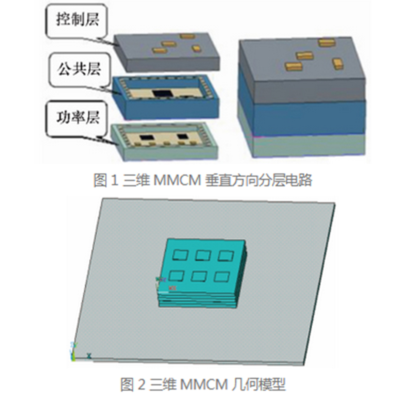
Fig. 2 3D MMCM
The temperature distribution of the 3D MMCM thermal simulation after thermal layout optimisation is shown in Fig. 3. As can be seen from the figure, the temperature distribution is uniform after the optimised layout, and the temperature step value is reduced accordingly, which ensures that the 3D MMCM works reliably within the permitted temperature range.
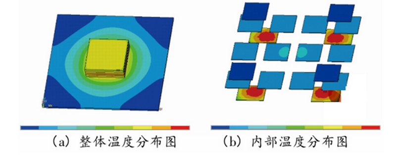
Fig. 3 Temperature optimisation distribution of 3D MMCM thermal simulation
2.LTCC High Precision Double-Sided Cavity Multilayer Substrate Manufacturing Technology
LTCC multilayer substrates with high-precision double-sided cavities are required to realise high-density interconnection and packaging of 3D MMCMs. In order to achieve this, on the basis of the existing LTCC multilayer substrate manufacturing process with single-sided cavities, we have broken through the technical difficulties in the stacking, laminating, and sintering processes of double-sided cavities. The double-sided cavity production process and the produced LTCC high-precision double-sided cavity multilayer substrate are shown in Fig. 4 and Fig. 5, respectively.
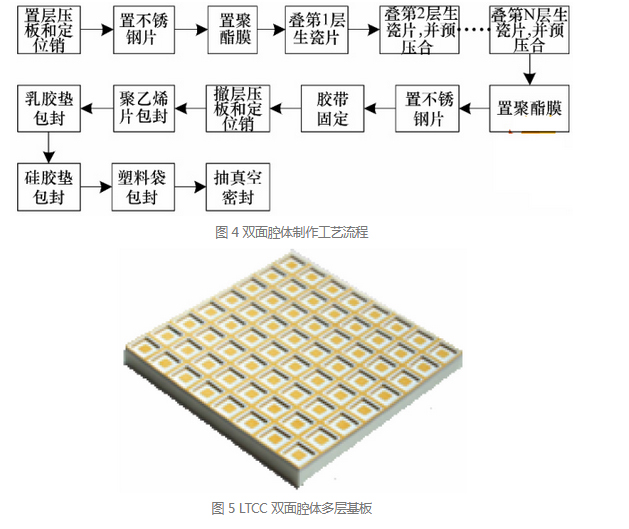
Fig. 5 LTCC Multilayer Circuit Substrate
In the double-sided cavity stacking process, the raw ceramic sheets are stacked in sequence, the neighbouring layers are pressed together by pre-pressing process, and polyester film and stainless steel sheet are placed on the surface layer after stacking, and the above technological measures better guarantee the accuracy of stacking alignment and the shape of the cavity. In the lamination process, the LTCC embryo after stacking is strengthened by pre-compression process to avoid the embryo moving or misalignment, and the filler in the cavity is also improved from the previous inserts to the elastic sealing material, which ensures the high precision of the double-sided cavity. In the sintering process, the speed of debinding and sintering is reduced to ensure the flatness and shrinkage of the LTCC multilayer substrate with single-sided cavities.
3.Vertical Interconnection of Microwave and Millimetre Wave Circuits
In MMCM,the key to form a three-dimensional structure is how to realise the vertical interconnection between the microwave millimetre wave circuits in each plane. At present, the main process methods to achieve vertical interconnection of microwave millimeter wave circuits include ball grid array (BGA) package interconnection and hairpin button interconnection.
3.1 BGA Package Interconnect Technology
BGA package interconnection is to make an array of solder balls at the bottom of the planar microwave millimetre wave circuit board as the I/O end of the circuit to interconnect with other planar microwave millimetre wave circuit boards or PCB main boards.BGA package interconnection has the following features.
1) High assembly density, the smallest ball diameter is 0.2mm,more connection points can be connected in the same area.
2) The contact surface between the array solder balls and the substrate is large and short, which is conducive to heat dissipation.
3) Array soldering ball pin is very short, shorten the signal transmission path,reduce the lead inductance, resistance, improve circuit performance.
4) Detection is difficult, only X-ray can detect the welding effect.Therefore,this technology can achieve high-density, high-performance vertical interconnection of planar microwave millimetre wave circuits.
Fig. 6 shows the application of BGA package technology to the millimetre wave LTCC module. Fig. 7 gives the simulation results of its S-parameter, which shows that the BGA package interconnect has a good performance as a microwave millimetre wave transmission medium.
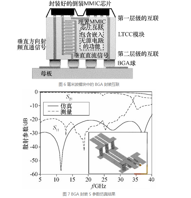
Fig. 7 BGA Packaging Technology
3.2 Fuzz Button Interconnection Technology
Fuzz Button is a very thin wire that is compressed into an elastic cylinder of a certain diameter and height through a mould of a certain shape. When the length of the Fuzz Button is pressurised, it will shrink, and when the pressure is removed, it will be restored, as shown in Fig. 8.

Fig. 8 Photograph of a typical hair button
The hairpin button has the following features.
1) Small structure size, favourable to signal integration.
2) Good microwave performance, wide operating bandwidth, up to 40GHz.
3) No soldering contact, easy to disassemble, low cost.
4) High current resistance, single-point current resistance 5A.
5) Anti-vibration and shock-resistant, long service life.
Therefore, the solderless connection technology of vertical interconnection using hairpin button connector has become one of the important technologies for 3D high-density packaging. Fig. 9 shows a 3D simulation model of the CST of the fabric interconnect circuit, in which the upper and lower circuits adopt the ribbon wire structure, and the interconnection of microwave and millimetre-wave signals is achieved through the fabric circuit structure in the middle. The fabricated button adopts a four-wire structure, with the middle button transmitting the RF signal and the surrounding three buttons forming a mask structure. The spacing between the three surrounding hairpin buttons and the middle hairpin button, and the spacing between the middle hairpin button and the bandwidth RF layer are set as the scanning parameters, and the final scanning simulation S-parameter curve results are shown in Fig. 10. From the figure, it can be seen that the performance of the hairy button as a microwave millimetre wave transmission medium is good.
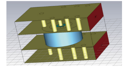
Fig. 9 Three-dimensional simulation model of the CST of the hairy button interconnection
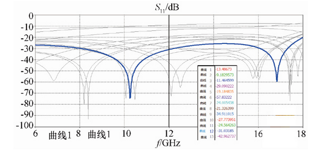
Fig. 10 Simulation result of S-parameter of hairy button
Comparing and analysing the above two new vertical interconnections, especially in simulating and analysing the microwave transmission performance, their interconnection structures have good microwave millimetre wave transmission performance. Due to practical applications, in addition to the transmission of microwave millimetre-wave signals, but also need to transmit a large number of control and power supply signals, often involving multiple points of interconnection at the same time, therefore, according to the actual use of the preferred use of the above radio frequency interconnection to achieve the microwave millimetre-wave signals, control signals and power signals to achieve the effective transmission.
4.3D MMCM sealed welding technology
The 3D MMCM needs to be sealed and welded together with a metal casing to ensure its long-term reliable operation, as shown in Figure 11.
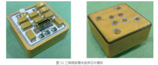
Figure 11 3D MMCM
3D MMCM Seal Welding consists of three main parts.
1) Welding between the power storage layer and the sealing ring.
2) Welding between power layer RF socket and base plate; 3) Welding between sealing ring and power layer base plate.
3) Welding between the sealing ring and the base plate of the power layer.
Due to the high density of 3D MMCM,the welding of the sealing ring should minimise the heat-affected area to avoid damage to the wafer and the previous welding joints, and the highly concentrated energy density of pulse laser welding is the ideal welding method; while the welding between the power storage layer and the sealing ring as well as the welding between the power layer RF sockets and the backplane can be realised by the electrode welding method. The sealing welding by pulse laser seam welding has the advantages of high airtightness,high joint strength, small heat-affected area,small thermal deformation,no mechanical stress and mechanical deformation, no contamination of welded joints, and high yield, which meets the requirements of sealing welding of sealing rings of three-dimensional MMCM and the base plate of power layer.
The 3D MMCM outer shell and cover plate are welded by laser welding to form a continuous dense weld to achieve the sealing airtightness requirements,so it is necessary to study the factors affecting the quality of sealing weld, including the weldability of the welded base materials, the structural design of the welded joints,plating,weld contaminants,the internal stresses of the materials,the parameters of the laser welding process, the welding method (welding sequence and the design of the workholding fixtures), etc., and finally find a reasonable laser welding seal.The final result is a reasonable laser welding sealing process.Since no welding material is added during the laser sealing welding process and the base material of the cover plate and shell is directly melted to form the weld pool, the weld structure of the cover plate and shell and the mating gap are very important.Therefore,the weld structure and fit-up gap of the cover and shell are very important. If the structure is not reasonable or the gap is large, the weld is prone to produce unfused defects.Fig.12 gives the optimised weld structure of a 3D MMCM seal.
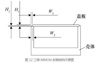
Fig.12 3D MMCM
By optimising the main welding process parameters such as peak laser power, welding speed, pulse repetition frequency, pulse width and defocusing amount, the laser welds were made dense and uniform, with an aesthetic appearance (as shown in Fig. 13) and no welding defects, and were confirmed to have met the requirements of the module airtightness indexes after fine leakage inspection by helium mass spectrometry and coarse leakage inspection by fluorine oil leakage tester.
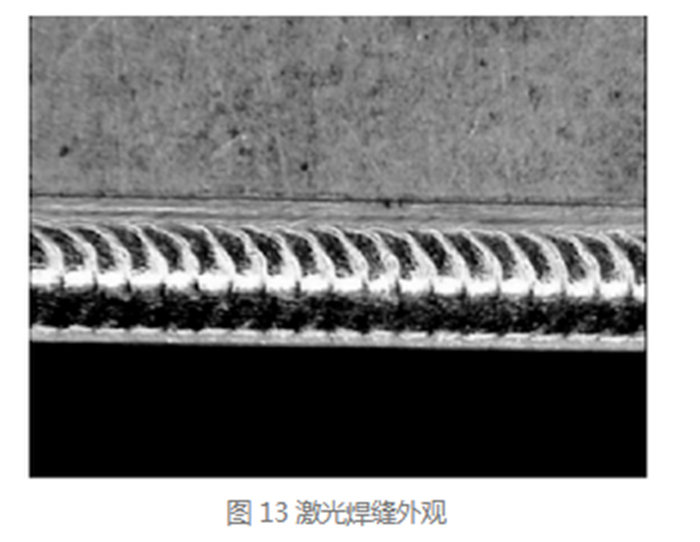
Fig. 13 laser (loanword)
Three-dimensional interconnection and packaging technology is the key technology for the development of miniaturised,highly integrated and reliable microwave millimetre wave active phased array antenna core MMCM.Through the development of 3D multi-layer multi-chip thermal layout optimisation design, the temperature distribution of MMCM is uniform and the value of sudden temperature change is reduced,which effectively solves the difficulty of efficient heat dissipation of 3D MMCM and ensures that the 3D MMCM works reliably within the permissible temperature range.On this basis,LTCC substrates with high-precision double-sided cavities are developed,and three-dimensional interconnection and packaging technologies such as ball grid array (BGA) and hairpin microwave millimetre wave vertical interconnection technology and laser sealing soldering technology are adopted to develop miniaturised, high-performance and highly reliable three-dimensional MMCMs,which meet the requirements of new-generation microwave millimetre wave active phased array antennas.