A Trustworthy PCB and Electronic Manufacturing Enterprise! Contact Us



A PCB RF shield is the small metal can you see soldered over the radio section of nearly every wireless board, and it is the everyday tool for board-level EMI shielding. It looks like the simplest line on the bill of materials. It is also one of the easiest parts to get wrong, and the mistakes usually surface late, in the EMC lab, when every fix means another board respin. This article covers how shields are chosen, how the pads and vias around them should be laid out, and what tends to go wrong in assembly.
Radio circuits are noisy neighbors. A power amplifier throws energy in every direction, an oscillator leaks harmonics, and a digital clock two centimeters away couples into anything with a high impedance. A metal wall between them reflects and absorbs most of that field, which is why a grounded RF shielding can is the standard fix. The word that matters is grounded. A can that touches the ground plane at only a few points behaves less like a wall and more like a slot antenna, and it can make emissions worse than having no shield at all.
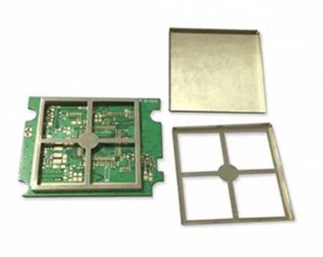
Shields come in a handful of styles, and the choice affects cost, assembly and repair more than it affects shielding performance. The cheapest option is a one-piece stamped can that goes down in reflow with everything else. If you need to get at the parts underneath, a frame with a snap-on lid is friendlier. For tight spaces, or for products that will be repaired often, a removable-lid [board level shielding] frame is usually the sensible compromise. Whichever you pick, decide early, because the footprint, the keep-out area and the pick-and-place setup all depend on it.
Before you add a can at all, ask what it is for. Shielding does two jobs. It keeps your own circuit from radiating enough to fail emissions tests, and it keeps a sensitive receiver, a GPS front end for example, from hearing the noise around it. Neither job replaces good layout. Short return paths, a solid ground plane and careful clock routing do most of the work, and the can handles what is left. We see designs that lean on the shield to rescue a messy layout. They usually end up with a more expensive board and still show a stubborn spike at one frequency.
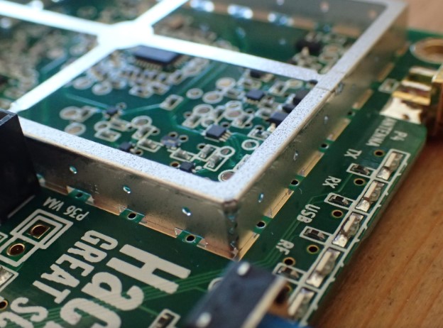
Materials are less exciting than they sound. Tin-plated steel is the cheapest, solders easily and does well at lower frequencies because of its magnetic properties. Nickel silver, a copper, nickel and zinc alloy, is the usual pick higher up the spectrum and where corrosion resistance matters. Stainless steel is tough but needs a solderable finish. Aluminum is light and hard to solder, so you mostly find it in lids and machined housings. Whatever the metal, ask for the plating thickness and the flatness of the solder edge. A wall that is only a tenth of a millimeter out of flat leaves a gap, and a gap leaks.
For products with several radio stages that must stay isolated from each other, a milled cavity shield with internal walls gives much tighter dimensions, at a higher price. Very thin modules sometimes skip the can and use a sprayed conductive coating over the package, which adds almost no height but needs a more specialized process.
The pad matters more than the can
Most shielding problems we hear about are really pad problems. For a PCB RF shield, the wall should land on a continuous copper pad, tied to the ground plane through a dense row of vias. That row, usually called a via fence, forms the lower half of the cage. A common rule of thumb is to space the vias no further apart than one twentieth of the shortest wavelength you care about. At 5 GHz the free-space wavelength is about 60 mm, which gives a ceiling of 3 mm, and plenty of designers go to 1 or 2 mm because harmonics of the radio can sit well above the operating band.
The copper pad should be a few tenths of a millimeter wider than the wall on each side, so a solder fillet can form and the placement machine has some forgiveness. Follow the shield maker’s recommended land pattern closely. Open the solder mask over the pad, and check that no stray mask covers part of it, since a half-masked pad makes an intermittent joint and an intermittent joint leaks.
Inside the can, keep components and traces back from the wall so nothing shorts to the metal, and leave extra room for the snap features on two-piece designs. Measure the tallest part under the shield and add margin for tolerance. A lid that presses on a component will crack a joint months later, and nobody will connect the failure to the shield.
Holes in a shield leak, more so as frequency rises. If you need vents for heat or flux outgassing, use several small holes in place of one large one. And think about signals that must leave the shielded area. They should cross at a planned point, ideally through a filtered feedthrough or a short inner-layer stripline, and not wander under the wall wherever the router finds space. A trace running beneath the wall carries noise straight past the barrier.
Heat gets trapped too
A shield is also a small oven. Power amplifiers and regulators under a can run hotter than they would in open air, so plan the thermal path early. Thermal vias under the hot part help. A thermal pad between the part and the lid can turn the metal into a heat spreader, though you should check that the pressure does not stress the part or the board. Leaving this until the first thermal test usually means moving the shield footprint, and by then the layout is full.
Assembly and rework
Shields normally go down with the same pick-and-place machine as the small parts, so they need tape-and-reel packaging and a flat top surface the nozzle can grip. Big cans have a lot of thermal mass. They can heat slowly or unevenly in reflow, which leads to a lifted edge or a joint that wetted on one side only. Check paste volume under the wall, confirm the reflow profile gives the can enough heat, and look at the first boards carefully. X-ray helps with hidden joints, since a closed top gives you nothing to see optically. Frame-and-lid designs are easier to inspect because the frame is open during soldering.
Rework deserves a thought from the start. Taking off a soldered can needs hot air or a dedicated station, and the neighboring parts see that heat as well. If the product will be repaired in the field, a frame and lid saves a lot of trouble, since a technician can lift the lid without desoldering anything.
Testing the result
Do not assume the shield works because it is there. A near-field probe and a spectrum analyzer will show leaks around the seam, the vias or any gap. Compare readings with and without the lid. A small pre-compliance chamber can tell you whether the product is likely to pass before you pay for a full test lab. If a hot spot appears at one frequency, look at the via spacing near it, check for a lifted solder joint, and review the size of any apertures.
Resonance is the one that surprises people. If the inside dimensions of the can match half a wavelength of a harmonic, the cavity rings and can make things worse. A small internal wall or a piece of absorber material usually damps it. The other usual suspects are a lid that does not seat fully at the corners, a wall that is slightly bent, and a via fence spaced too wide for the highest frequency that matters. Most of these are cheap to fix on screen and expensive to fix on a built board, which is the best argument for a design review before layout is frozen.