A Trustworthy PCB and Electronic Manufacturing Enterprise! Contact Us



The frequency synthesizer circuit board forms the core local‑oscillator hardware for wireless communication, radar, test‑and‑measurement and aerospace‑grade devices, drawing steady sourcing demands from global system integrators, RF engineering firms and technology OEM customers. As a China‑based PCB manufacturer focused on foreign‑trade high‑frequency projects, we collaborate regularly with overseas engineering teams on prototype validation and serial production for PLL‑based RF subsystems. Many hardware designers deliver solid simulation results in EDA software yet encounter unexpected phase‑noise drift, signal reflection or insertion‑loss degradation after physical fabrication. These performance gaps often trace back to poor stack‑up definition, material mis‑selection or insufficient impedance tolerance on the frequency synthesizer circuit board. For international buyers, understanding critical RF‑PCB manufacturing constraints improves technical communication, cuts iteration cycles and prevents costly production rework.
Unique Manufacturing Challenges for Frequency Synthesizer PCBs
A frequency synthesizer generates stable, tunable RF clock signals relying on PLL chips, VCO units, loop‑filter networks and auxiliary digital control logic. Unlike conventional consumer‑electronics PCBs, these boards operate at GHz‑range frequencies, where minor manufacturing deviations directly degrade key metrics including phase noise, spurious suppression and return loss. Standard FR‑4 material generally fails high‑frequency requirements due to high dielectric loss and unstable Dk value across temperature shifts. Most functional designs call for low‑loss laminates such as Rogers, Taconic or hybrid FR‑4/RF stack‑up configurations to maintain consistent electrical performance.
During our pre‑production DFM review for overseas customers, our RF engineering team pays extra attention to mixed‑signal partitioning. On a typical frequency synthesizer circuit board, sensitive analog RF traces sit side‑by‑side with fast digital control lines for I2C or SPI interfaces. Without thoughtful layout guidance, digital switching noise couples into PLL reference paths and elevates phase‑noise floor, ruining spectral purity of output signals. Our DFM feedback covers practical recommendations: physical separation between RF and digital zones, complete ground fencing around critical PLL‑VCO signal paths, optimized placement of decoupling capacitors near synthesizer IC power pins, and proper via‑fence implementation close to SMA connector landing areas. These low‑cost manufacturing‑side suggestions significantly reduce prototype failure risks for RF development teams.
Material and stack‑up specification represents another high‑impact decision point. Simple low‑frequency synthesizer prototypes may work with modified high‑Tg FR‑4. For applications above 1 GHz, however, designers need laminates with tightly‑controlled dielectric constant and low dissipation factor. Hybrid stack‑up schemes, combining RF substrate on signal layers and low‑cost FR‑4 for core layers, help overseas buyers balance RF performance against total bill‑of‑material expense. Regarding surface finish, ENIG is preferred for most RF synthesizer boards. It delivers flat, uniform pad geometry, preserves soldering reliability for fine‑pitch PLL and VCO chips, and avoids surface unevenness that disturbs high‑frequency transmission‑line impedance. Our sales‑engineering team evaluates each project’s operating frequency, environmental requirements and budget to propose practical material combinations for every overseas order.
From RF Prototype to Volume Production for Global Clients
Most RF synthesizer projects follow a standard workflow: schematic capture and PCB layout → prototype validation → small‑batch trial run → mass‑production deployment. As a foreign‑trade‑oriented high‑frequency PCB supplier, we support the full‑order chain, from quick‑turn bare‑board prototyping up to large‑volume serial manufacturing, serving startup RF firms, test‑equipment builders and established telecom OEMs worldwide.
Prototype iteration is essential for frequency synthesizer hardware. Even well‑simulated layouts may show phase‑noise drift, spurious outputs or impedance mismatch after fabrication. Our fast‑turn RF‑PCB service helps overseas engineers receive physical boards within competitive lead‑times for assembly, S‑parameter testing and spectrum‑analyzer validation. Once prototypes pass lab measurement, customers can smoothly transition toward small‑batch or mass production without redesigning existing Gerber and drill datasets.
Layer‑count selection depends largely on operating frequency and system complexity. Two‑layer constructions fit some cost‑limited sub‑GHz synthesizer demos. Real‑world tunable PLL systems for communications, radar or instrumentation mostly adopt 4‑layer or 6‑layer stack‑ups, assigning dedicated inner ground and power planes to isolate RF signal paths from power‑supply noise. During technical audit, our engineers verify trace width, trace spacing, annular ring, anti‑pad dimension and drill features against actual process capability. We flag manufacturability risks early, such as ultra‑fine RF traces, uncontrolled impedance segments or inadequate clearance around high‑frequency vias that would lower mass‑production yield.
We also handle replacement and form‑fit redesign orders for legacy test‑instrument modules widely used among North American and European technology maintenance vendors. In these cases, the frequency synthesizer circuit board must strictly replicate original outline dimensions, mounting holes and connector footprints to fit existing mechanical enclosures. Meanwhile we apply modern high‑frequency fabrication parameters to fix known weaknesses of older hardware, including unstable dielectric materials and insufficient ground shielding.
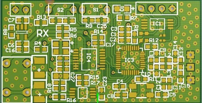
Common Sourcing Pain‑Points for International RF PCB Buyers
Years supporting RF foreign‑trade projects allow us to summarize typical obstacles customers face while sourcing frequency‑synthesizer‑related PCBs. Clarifying specifications before placing orders avoids most technical headaches.
Impedance deviation ranks among the top complaints. For RF synthesizer circuits, 50‑ohm controlled impedance is standard for signal transmission lines. Lamination thickness fluctuation, trace‑width etching tolerance and copper‑foil variation during production will shift real‑world impedance away from simulation values. Our factory supports TDR impedance testing with test‑coupon samples; for high‑end batches we offer 100 % impedance inspection to keep deviation within ±3 % as required by most RF system standards.
Phase‑noise degradation caused by crosstalk and insufficient shielding creates heavy trouble for multi‑channel synthesizer boards. Adjacent RF traces running in parallel without ground isolation bring signal coupling and unwanted spurious components. Our DFM workflow reminds customers to shorten critical RF traces, increase spacing between different signal channels and deploy ground‑via fences around sensitive transmission lines.
Mechanical and environmental reliability deserves special attention too. Many frequency synthesizer circuit boards end up inside outdoor telecom cabinets, field‑deployed radar units or laboratory test instruments experiencing wide temperature swings and continuous vibration. SMA connector pads and high‑density component landing areas need reinforced copper treatment to prevent pad lifting or trace fracture under long‑term operation. Our pre‑production review marks these high‑stress zones for extra attention.
Flexible order volume remains another key requirement for most overseas RF buyers. Synthesizer projects frequently require small prototype quantities, mid‑volume trial batches and later‑stage scaled‑up mass production. We accept flexible batch‑size demands for high‑frequency PCB orders. For export shipments we supply complete commercial documents, support AOI, impedance and S‑parameter‑related testing upon request, and cooperate with multiple international shipping solutions delivering goods to North America, Europe, Southeast Asia and other destinations.
File Preparation Guidance for Your RF Synthesizer PCB Order
Sufficient document preparation accelerates project progress when collaborating with Chinese high‑frequency PCB manufacturers. Please submit complete Gerber files, drill files, detailed layer‑stack‑up definition, laminate‑material specification, target impedance values, copper‑thickness requirement, surface‑finish choice and order quantity. If you have special RF‑related demands such as phase‑noise‑oriented layout constraints or environmental operating‑range limits, note these clearly within order instructions.
If your engineering team lacks extensive high‑frequency layout experience, you may share schematics and stack‑up sketches for our free‑of‑charge DFM feedback service. Our team points out potential manufacturability and RF‑performance risks, though full PCB layout design is not covered within this service scope. Clear two‑way technical communication reduces revision loops and helps control total project expenditure.
Market Outlook for RF Frequency Synthesizer Hardware
Global market demand for RF and microwave hardware keeps expanding. 5G infrastructure expansion, new‑generation radar equipment, software‑defined radio and portable test‑and‑measurement devices continuously generate new procurement opportunities for specialized high‑frequency printed‑circuit boards.
Most general‑purpose PCB factories only accumulate experience with FR‑4‑based consumer electronics; they lack mature process parameters for low‑loss RF laminates and tight‑tolerance impedance control. Selecting a supplier familiar with frequency‑synthesizer‑specific manufacturing characteristics directly improves finished‑product yield and final spectral performance. Whether you develop new PLL‑VCO subsystems, produce communication radio modules or deliver replacement boards for legacy test instruments, professional PCB manufacturing support helps your RF hardware stay competitive on global markets.
Conclusion
A well‑fabricated frequency synthesizer circuit board serves as the physical foundation for stable, low‑phase‑noise local‑oscillator signals inside modern RF equipment. For foreign‑trade purchasers in wireless and test‑measurement industries, sourcing the frequency synthesizer circuit board means more than purchasing bare printed‑circuit hardware. It means gaining access to professional RF‑oriented DFM engineering review, flexible high‑frequency production capacity and full‑set export‑oriented services. Fully considering high‑frequency manufacturing requirements and maintaining smooth technical dialogue with your PCB vendor minimizes unexpected failures and speeds‑up time‑to‑market for your radio‑frequency products across the world.