Backdrill PCB is a circuit board that uses the controlled depth drilling method to drill off the Stub hole wall of the connector through-hole or signal through-hole using the secondary drilling pipeline.
As shown in the figure below, after the through-hole is shaped, the excess Stub of the PCB through-hole is removed through secondary drilling from the back, of course, the diameter of the Backdrill drill bit should be larger than the through-hole hole diameter,and according to the processing of the depth of drilling process tolerance level in the PCB holes can not be damaged on the basis of connecting the PCB holes and alignments to ensure that the length of the remaining Stub is as small as possible, that is, the so-called controlled-depth drilling.
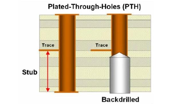
Through-hole BackDrill Schematics
The above diagram shows the BackDrill profile of the through-hole: the left side is the normal signal through-hole; the right side is the diagram of the through-hole after Backdrill, which indicates that the through-hole is drilled from the Bottom layer all the way to the signal layer where the alignment trace is located.
Backdrill technology removes the parasitic capacitance effect caused by the stub on the hole wall and ensures that the impedance of the through-hole in the channel link is consistent with that of the alignment, which reduces signal reflection and improves signal quality.
Backdrill is one of the most cost-effective and efficient technologies for improving channel transfer performance. The use of backdrill technology will have a certain increase in PCB manufacturing costs.
Classification of Single Board Backdrill
There are two types of back drilling: single-sided back drilling and double-sided back drilling.
Single-sided drilling can be divided into drilling from the TOP side or from the BOTTOM side. The PIN holes of connector inserts can only be back-drilled from the side opposite to the side where the connector is located. When both TOP and BOTTOM sides of the PCB are equipped with high-speed signal connectors, double-sided back-drilling is required, as shown below.
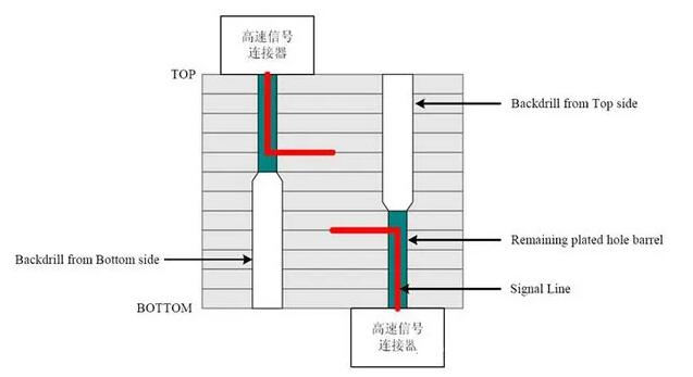
Double Sided Back Diamonds
Because of the accuracy of backdrill depth control, the industry's current capability can reach ±4mil, and the capability of Chinese suppliers can reach ±6mil. In order to improve reliability, it is better to keep some redundancy in the design, and it is recommended to meet the following design requirements.
BackDrill rules in PCB design
1) ‘Remaining hole wall length’ of PCB holes for crimp connectors.
In the figure below, the requirement is: L≥L1+12mil.
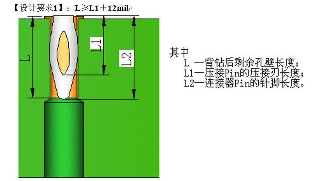
BackDrill Remaining Hole Wall Length
Based on the above relationship, the minimum remaining hole wall requirements for the different connector cross-holes can be derived.
It should be noted that the L1 tolerance for the crimp edge length of the 2mm connector is slightly larger, so it is slightly relaxed when determining the L length.
2) Backdrill Depth Control
Backdrill depth control is recommended to keep at least 8mil of Stub,in the layer setting needs to take into account the thickness of the media, to avoid the occurrence of the alignment is drilled off the situation. Backdrill depth control is recommended between two layers, the thickness between the two layers is required to be ≥12mil.
For example: back drilling hole 1, when the distance between two adjacent layers (such as L12/L13, L13/L14) does not meet ≥ 12mil, and L12/L14 layer spacing ≥ 12mil, it is recommended that the depth of back drilling holes in the L12/L14; back drilling holes 2/3, when the distance between the L9/L10 layer spacing ≥ 12mil, it is recommended that the depth of back drilling holes in the L9/L10 between the control.
3) PCB alignment to back-drilled hole spacing
The distance from the PCB alignment to the edge of the back-drilled hole is ≥10mil.
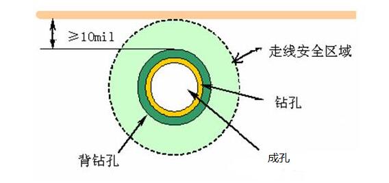
PCB alignment to back-drilled hole spacing
4) Back drilling hole diameter size
Back-drilled hole diameter (D) = drilled hole diameter (d) + 10mil
Back-drilled holes are ≥ 0.25mm from the inner graphic recommendation and ≥ 0.3mm from the outer graphic recommendation.
The distance from the back drill hole to the back drill hole is ≥0.25mm.
5) Back-drilled hole welding disc design requirements
There is no copper ring left after back-drilling of the cross-hole welding disc.
In order to recommend the back-drilled hole welding discs, the following design is required:
Welding disc on the back-drilled side ≤ diameter of the back-drilled hole;
The inner layer pads are recommended to be designed as a trayless process.
6) Back-drilling PCB surface processing technology
The surface finish of the back-drilled PCB requires the use of OSP or chemical immersion tin, and HASL is prohibited;
Non-functional pads on the inner layer of the PCB are designed to be tray-less.
Add text in Smartdrill layer: NO FUNCTIONAL PADS ON INTERNAL SIGNAL LAYERS MUST
BE REMOVED.
Tips:Backdrilled holes and backdrilled surfaces cannot be used for ICT testing at the same time.
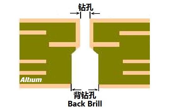
Backdrill
How high a signal rate should Backdrill PCB process be applied in PCB design?
The general understanding is that signals ≥ 5Gbps need to be considered for Backdrill PCB design.
Of course, the design of high-speed interconnect is a systematic project. If the chip driving capability is strong enough, or the system interconnect is not so long, the signal quality may still pass without Backdrill design. Therefore, the most reliable way to determine whether a Backdrill PCB is needed is to simulate the system interconnect.