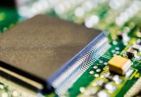
In the fast-developing electronics industry, the importance of packaging technology as a key link between the chip and the circuit board is self-evident. Among them, Ball Grid Array (BGA) packaging technology and Surface Mount Technology (SMT) as a high-density, high-performance packaging methods,has been widely used. In this paper, we will discuss the BGA packaging process and its combination with SMT placement technology, how to realize high-density, high-performance electronic systems.
First,BGA packaging process analysis
1.Technical background and characteristics
BGA packaging technology was launched by Intel in 1991, and was widely used in 1993. This packaging method by forming a regular ball-shaped pin array at the bottom of the package, effectively reducing the process size and chip area, while maintaining good performance and reliability.The main features of BGA packaging include:
(1) high-density pins: BGA package by increasing the connection point of the metal leads and external cables to improve the link density and reduce the size and weight of the package. Its pin spacing is larger to achieve a higher number of I / O pins to meet the needs of high-performance integrated circuits.
(2) Excellent signal transmission performance: Due to the short connection path of the solder balls, the BGA package has low parasitic inductance and capacitance, which is conducive to high-speed signal transmission.
(3) High reliability: the use of tin ball fixed connection, not only patch is convenient, but also effectively protect the component leads to prevent oxidation and extend the service life of components.
(4) easy to automate production: BGA packaging process can be automated mechanical assembly, improve production efficiency and reduce production costs.
2.The main process
The main process of BGA encapsulation includes the production of solder balls, substrate production, chip paste, encapsulation curing and slitting package and other steps:
(1) Solder ball production: the use of high-purity tin-lead alloy or lead-free materials to produce solder balls, forming a regular ball-shaped pin array.
(2) substrate production: the use of multi-layer printed circuit board (PCB) as a substrate to achieve high-density, high-performance electrical interconnection.
(3) Chip Pasting: The chip is attached to the substrate and connected to the substrate by lead-free or leaded solder.
(4) Encapsulation and curing: Epoxy resin is used to encapsulate the chip and protect it from environmental influences.
(5) Slitting package: cut the encapsulated chip into individual BGA packages.
3.Welding and quality control
BGA welding is usually reflow soldering technology, need to strictly control the welding temperature, time and furnace temperature curve to ensure the welding quality. After welding, quality inspection, such as X-ray inspection and acoustic emission inspection, is also required to detect welding defects and ensure the reliability of the connection. For poorly welded BGA package, special repair equipment can be used to re-weld.

BGA
Second, SMT placement technology in the realization of high-density, high-performance
1. SMT technology overview
SMT is a technology that mounts electronic components directly onto the surface of a circuit board, allowing the use of smaller components to achieve higher package density. the key to SMT is the use of solder paste, applied to the circuit board by printing or drop-coating, and then heated in a reflow oven to fix the components.
2. High Density Realization
SMT SMD technology realizes high density packaging through the following ways:
(1) Miniature components: SMT technology allows the use of smaller sized components, such as 0201, 01005, and other miniature packages, thus increasing the component density of the board.
(2) Multi-layer circuit boards: The use of multi-layer circuit board design allows for more electrical interconnections in a limited space, further increasing the density of the package.
(3) Advanced layout and wiring: Through optimized design, the layout and wiring of components are reasonably arranged to reduce space waste and improve packaging efficiency.
3. High performance realization
SMT placement technology realizes high performance through the following ways:
(1) Accurate placement process: master the precise placement process, including placement speed, placement pressure, placement temperature and other parameters of the precise control, to ensure the accurate placement of components, reduce placement errors and defective products.
(2) Advanced welding technology: using reflow soldering, wave soldering and other advanced welding technology to ensure the stability and consistency of welding quality.
(3) Strict quality control: the implementation of strict quality control procedures, including the first piece of inspection, process testing and finished product inspection, to ensure product quality in line with design requirements and production process standards.

BGA
Third, the combination of BGA and SMT applications
The combination of BGA packaging technology and SMT placement technology provides an efficient and reliable solution for the field of electronics manufacturing. Through the BGA package to achieve high-density pins and excellent signal transmission performance, combined with the SMT placement technology of high precision and automated production advantages, you can produce high-performance, high-reliability electronic products.