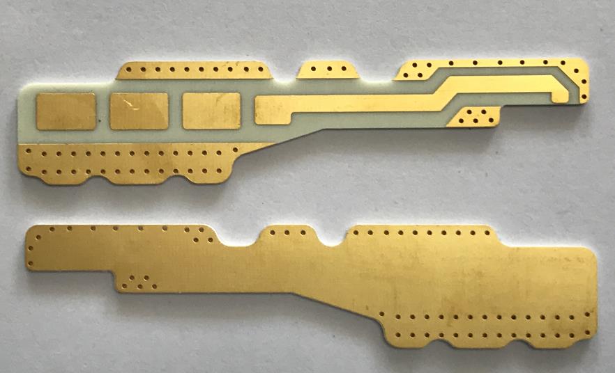
The release of gases from materials is a problem worth investigating for any electronic equipment intended for use in a high vacuum environment. The term ‘degassing’ refers to the release of gases trapped inside solid materials such as high-frequency circuit board materials.With the rapid development of aerospace (space-based field), 5G applications, medical systems and other industries, more and more fields are beginning to pay attention to the de-gassing characteristics of the material,and put forward special requirements for the quota. In space-based equipment, gases released from materials can condense on equipment such as camera lenses, rendering them inoperable. Hospitals and medical organisations must also exclude potentially outgassing materials to ensure a sterile environment.
Under absolute vacuum conditions, degassing (also known as outgassing) of materials can lead to a reduction in the performance of charge-coupled device (CCD) sensors in space probes. This has prompted NASA to develop rigorous procedures for evaluating materials for outgassing before they are used in vacuum applications. For example, NASA test programme SP-R-0022A is used to test composite materials such as circuit board circuit board materials. ASTM International, a leading materials standards organisation, has published a number of related standards (e.g. ASTM E595-07) to measure certain key parameters of materials, such as Total Mass Loss (TML), Collected Volatile Condensable Material (CVCM), in order to evaluate various changes in the performance of different materials as a result of degassing in a vacuum environment. NASA's Goddard Space Flight Center (GSFC) has long supported a policy of selecting materials with the lowest outgassing rates as the preferred materials for spacecraft and space applications. Testing is conducted in accordance with the ASTM E595-07 standard, which outlines a test method for evaluating the change in mass of a specimen over a 24-hour period at +125°C under vacuum conditions. The target number of NASA-acceptable TMLs is less than 1%, and the target number of CVCMs is less than 0.1%.
The use of the term vacuum in these tests is somewhat subjective.According to the standard,tests are not necessarily conducted at absolute vacuum levels,and typical values for vacuum are usually 10-12 Pa (10-14 Torr). In practice, the standards used by ASTM only specify that the vacuum level for TML and CVCM testing at +125°C for 24 hours should be less than 7 x 10⁻³ Pa (5 x 10⁻⁵ Torr). Tests are usually conducted at temperatures at least +30°C above typical operating temperatures in order to accelerate the realisation of the material's service life.

High Frequency Circuit Board
According to the test standard, after 24 hours of vacuum/high temperature testing, the specimen should be weighed again at +23°C and 50% relative humidity to minimise the effect of water vapour on the accuracy of the measurement. During the 24-hour heating period, the specimens are placed in glassware and must be weighed within 2 minutes of opening the glass vials to minimise the loss of water vapour uptake from exposure to uncontrolled humidity. Additional testing for water vapour recovered (WVR) can be performed after measurements of TML and CVCM. The test can be carried out with the material in its original state or in a cured state.
Low levels of outgassing are usually associated with high quality materials and well-controlled manufacturing techniques. For example, a variety of circuit board materials from ROGERS Corporation have been tested in accordance with NASA test procedure SP-R-0022A for TML, CVCM, and WVR, and these families of materials have been shown to be well suited for spacecraft applications. These materials include RT /duroid ® composites based on PTFE resins and inorganic fillers (e.g., glass or ceramic fillers, etc.), as well as the TMM ® family of temperature-stabilised hydrocarbon composites.Prior to testing according to SP-R-0022A, samples are etched to a copper-free condition and heated under vacuum at +125°C for 24 hours. Samples were 100 to 300 mg in size and placed in copper housings.The outlet ports of each housing were heated to +125°C while the chrome-plated collector was kept at +25°C with a distance of 12.7 mm from the outlet.
For these tests, the TML and CVCM test data for RT/duroid and TMM circuit board materials were impressive in all cases, with NASA's maximum recommended values of 1.0% and 0.1%, respectively, and for RT/duroid 5880, a laminate with PTFE resin, glass fibre filler, and a relative dielectric constant of 2.20, the TML and CVCM values are 0.03% and 0.00% respectively.The TML and CVCM values of the RT/duroid6002 circuit board material were 0.02% and 0.01% respectively, which was also based on a PTFE resin system but with a lower concentration of glass microfibre and ceramic fillers and a relative dielectric constant of 2.94.
For all RT/duroid and TMM materials tested, the TML values were well below 0.1% and the CVCM values were equal to or close to zero. TMM circuit board materials are highly crosslinked thermoset hydrocarbon materials characterised by low TML and CVCM values. TMM 3 circuit board material has a relative dielectric constant of 3.27, a TML of 0.04% and a CVCM of 0.00%. The TMM 10 circuit board material with a higher dielectric constant of 9.20 had a TML value of 0.06% while maintaining a CVCM of 0.00%. The largest TML value of all the materials tested was for 3001 semi-cured sheet, a thermoplastic chlorofluorocarbon copolymer with a relative dielectric constant of 2.28, designed for bonding multiple PTFE-based circuit boards to form multi-layer circuits. Despite this, its TML test value was only 0.13 per cent, well below NASA's upper limit of 1.0 per cent, and the CVCM was only 0.01 per cent, one-tenth of the maximum value recommended by NASA.
Although circuit board material outgassing is not a substantial concern for all circuit design engineers, material outgassing is not an easy task for those working on satellites and other aerospace electronics. The most prudent approach to circuit board materials is to select materials with the lowest possible TML, CVCM and WVR values.