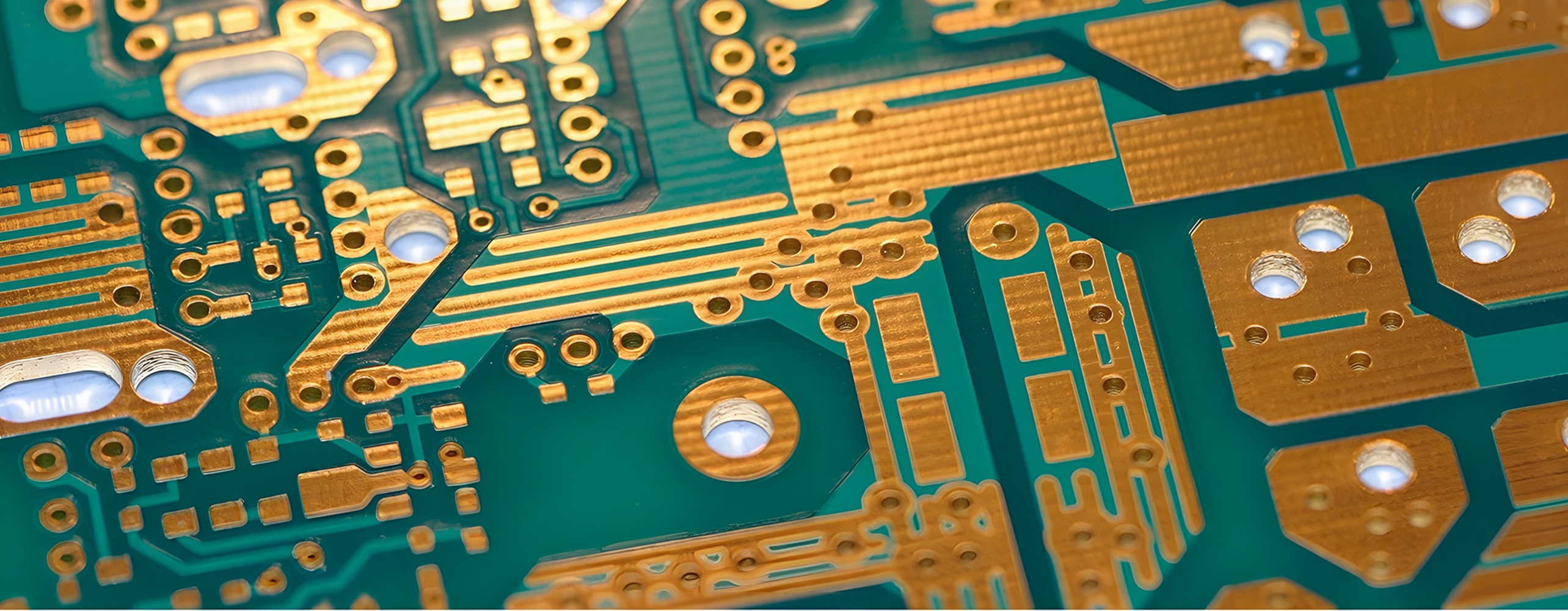
Electroless Nickel Immersion Gold (ENIG) plating is a widely adopted surface finish in the PCB (Printed Circuit Board) industry, known for its excellent conductivity, corrosion resistance, and reliability. ENIG plating consists of two layers: an underlying nickel layer and an upper layer of gold.
The nickel layer acts as a barrier to the copper beneath, while the gold layer protects the nickel and offers a solderable surface. This article delves into the process, benefits, applications, and potential challenges of ENIG plating in PCB manufacturing.
The ENIG Plating Process
The ENIG plating process is complex and involves multiple steps to ensure that the PCB meets the necessary standards for performance and durability. Here’s a breakdown of the main stages:
Cleaning: The PCB surface is cleaned to remove any contaminants such as grease, dust, or oxidation that may interfere with the plating process.
Micro-etching: A light etching is done to roughen the surface of the copper, which enhances the adhesion of the nickel layer.
Pre-treatment: The board is treated with a solution that prepares the copper surface for the nickel deposition.
Nickel Plating: The board is immersed in an electroless nickel bath, where a chemical reaction deposits a uniform layer of nickel on the exposed copper surfaces. The thickness of the nickel layer is usually between 3 to 6 microns.
Gold Immersion: After nickel plating, the board is placed in an immersion gold bath, where a thin layer of gold, typically between 0.05 to 0.1 microns, is deposited on the nickel layer through a displacement reaction.
Final Rinse and Drying: The PCB is thoroughly rinsed to remove any residues from the plating baths and then dried.

ENIG Plating: An Essential Surface Finish
Advantages of ENIG Plating
ENIG plating is favored in PCB manufacturing for several reasons, particularly in high-reliability applications where performance is critical. Here are some of the key advantages:
Excellent Surface Planarity: ENIG plating offers a flat surface, making it ideal for fine-pitch components, ball grid arrays (BGAs), and surface-mount technology (SMT). The planarity ensures reliable soldering and minimizes the risk of defects such as bridging or tombstoning.
Superior Corrosion Resistance: The nickel layer in ENIG plating acts as a robust barrier, protecting the underlying copper from oxidation and corrosion. This is especially important in harsh environments where the PCB may be exposed to moisture, chemicals, or extreme temperatures.
Good Solderability: The gold layer in ENIG provides an excellent solderable surface, which is crucial for ensuring strong and reliable solder joints. Unlike other surface finishes, ENIG maintains its solderability over time, making it suitable for long-term storage and use.
Wire Bonding Compatibility: ENIG is compatible with both aluminum and gold wire bonding, which is essential for certain applications, such as in semiconductor packaging and high-frequency circuits.
Lead-Free Compliance: As the electronics industry moves towards lead-free manufacturing due to environmental regulations, ENIG plating stands out as a lead-free option, complying with RoHS (Restriction of Hazardous Substances) directives.
Applications of ENIG Plating
Due to its excellent properties, ENIG plating is widely used in various applications across different industries:
Consumer Electronics: ENIG is commonly used in the manufacturing of smartphones, tablets, laptops, and other consumer electronic devices where high reliability and performance are required.
Automotive Electronics: In the automotive industry, PCBs with ENIG plating are used in critical systems such as engine control units (ECUs), infotainment systems, and advanced driver-assistance systems (ADAS).
Medical Devices: ENIG plating is also prevalent in medical devices that require high levels of reliability, such as diagnostic equipment, implantable devices, and monitoring systems.
Aerospace and Defense: In aerospace and defense applications, where PCBs must withstand extreme conditions, ENIG plating provides the necessary durability and performance.
Telecommunications: ENIG is used in the manufacturing of PCBs for telecommunications equipment, including routers, switches, and base stations, where signal integrity and reliability are paramount.
Challenges and Considerations
While ENIG plating offers numerous advantages, there are also challenges and considerations that manufacturers must address to ensure optimal results:
Cost: ENIG plating is generally more expensive than other surface finishes due to the cost of materials, particularly gold, and the complexity of the process. However, the benefits often outweigh the costs in high-reliability applications.
Black Pad Defect: One of the most significant challenges with ENIG plating is the potential for black pad defect, a form of corrosion that occurs between the nickel and gold layers. This defect can lead to solder joint failures, particularly in fine-pitch components. Strict process control and regular inspection are essential to minimize the risk of black pad defect.
Thickness Control: Achieving the correct thickness of the nickel and gold layers is crucial for the performance of the PCB. Variations in thickness can affect solderability, wire bonding, and overall reliability. Manufacturers must ensure precise control over the plating process to meet specifications.
Environmental Considerations: The chemicals used in the ENIG plating process, such as nickel and gold salts, can have environmental impacts if not handled properly. Manufacturers must adhere to environmental regulations and implement proper waste management practices to minimize these impacts.
Complexity of Process: The ENIG plating process is more complex than other surface finishes, requiring careful monitoring and control of various parameters. This complexity can increase production time and requires specialized knowledge and equipment.
ENIG plating remains a critical surface finish in the PCB industry, offering a balance of performance, reliability, and versatility. Despite its challenges, such as cost and potential defects, the advantages of ENIG plating make it the preferred choice for many high-reliability applications. As the industry continues to innovate, we can expect further improvements in the ENIG process, ensuring that it remains a cornerstone of PCB manufacturing for years to come.