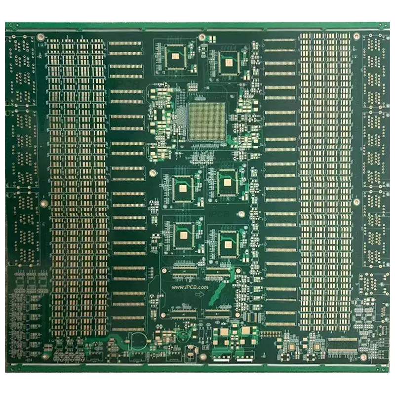

Product Name: High Speed PCB
Substrate: Panasonic Megtron6 (M6)
Layer: 16L
Finished thickness: 1.2mm
Copper thickness: 1/H/H/1oz
Minimum line width/spacing: 4mil/4mil
Surface treatment: ENIG
Minimum mechanical hole: 0.2mm
Laser blind hole: 0.1mm
Product application: Communication equipment
Among PCB types, high-speed PCB play a crucial role in the field of high-speed circuit due to their unique performance advantages. So, what is high-speed PCB?
High speed PCB is a printed circuit board designed specifically for high-speed circuit. It uses special materials and processes to achieve high-speed signal transmission and low latency. In high-speed circuit applications, the transmission speed and quality of signals are crucial to the performance of the system, and high-speed PCB were born to meet this demand.
High frequency PCB is mainly used for high-frequency (above 1GHz) and ultra-high frequency (above 10GHz) electronic devices, such as RF chips, microwave receivers, RF switches, vacancy tuners, frequency selective networks, etc. Unlike high-frequency PCB, designing high-speed PCB requires more consideration of factors such as signal integrity, impedance matching, signal coupling, and signal noise. In order to meet these requirements, high-speed PCB require the use of special materials and processes. In high-speed PCB design, selecting suitable high-speed CCL materials is crucial. Data center switches and AI servers are important application areas for high-speed PCB board. AI servers typically have features such as large memory and high-speed storage, multi-core processors, and require PCB specifications and performance to match them. The mainstream data center switch port speeds are evolving from 10G/40G to 400G/800G.
What are the advantages of high-speed PCB compared to standard PCB?
1. High speed PCB have high-speed transmission performance. High speed PCB use materials with low loss and high frequency characteristics, which can ensure the speed and stability of signals during transmission, reduce signal distortion and delay.
2. High speed PCB have excellent heat dissipation performance, and high-speed circuit generate a large amount of heat during operation. Through optimized design and material selection, high-speed PCB have good heat dissipation performance, ensuring the stable operation of the circuit board.
3. High speed PCB have low dielectric constant and low dielectric loss, which are important indicators for measuring the performance of circuit boards. High speed PCB use materials with low dielectric constant and low dielectric loss, which can effectively reduce signal loss during transmission and improve signal transmission efficiency.
4. High speed PCB have good mechanical and processing properties. High speed PCB not only have excellent electrical performance, but also good mechanical and processing properties, making production and installation convenient.
High speed PCB are widely used in communication, computer, server, automotive electronics, medical equipment and other fields, providing reliable technical support for high-speed data transmission and low latency requirements in these areas.
Choosing high-quality high-speed PCB is also crucial. High quality high-speed PCB not only ensure stable signal transmission, but also improve equipment reliability and lifespan. Therefore, when choosing high-speed PCB, we need to comprehensively consider factors such as performance, quality, and cost, and choose the product that best suits our needs.
As a key component of high-speed circuit, the performance and quality of high-speed PCB have a significant impact on the overall operation of the system. Understanding the important information of high-speed PCB and choosing high-quality products will help improve the performance and stability of equipment, and promote the continuous development of electronic technology.
Product Name: High Speed PCB
Substrate: Panasonic Megtron6 (M6)
Layer: 16L
Finished thickness: 1.2mm
Copper thickness: 1/H/H/1oz
Minimum line width/spacing: 4mil/4mil
Surface treatment: ENIG
Minimum mechanical hole: 0.2mm
Laser blind hole: 0.1mm
Product application: Communication equipment
iPCB Circuit provides support for PCB design, PCB technology, and PCBA assembly. You can request technical consultation or quotation for PCB and PCBA here, please contact email: sales@ipcb.com
We will respond very quickly.