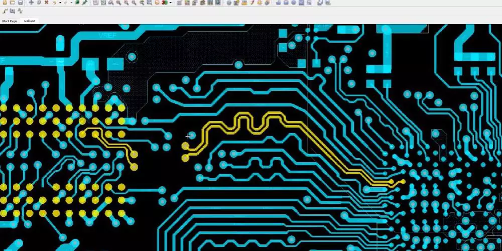
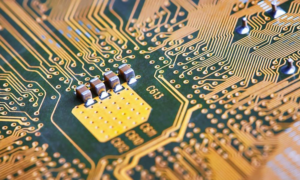
As the output switching speed of integrated circuits increases and the density of PCB boards increases, signal integrity (SI) has become one of the issues that high speed PCB design must be concerned about. Factors such as component and PCB parameters, component layout on the PCB, and high-speed signal routing can all cause high-speed signal integrity problems, resulting in unstable or even non-functional systems.
With the high-speed development of the times, more and more products and systems need to face more and more stringent performance requirements and an increasing amount of data processing, which prompted the high-speed PCB design has gradually become one of the advanced skills that must be mastered by the current PCB engineers.

high-speed PCB design
Good high-speed signal integrity means that the signal responds with the correct timing and voltage level values when needed. Conversely, a signal integrity problem occurs when the signal does not respond properly.
High-speed signal integrity problems can cause or directly contribute to signal distortion, timing errors, incorrect data, address and control lines, and system malfunctions and even system crashes.
PCB high-speed signal integrity problems mainly include signal reflection, crosstalk, signal delay and timing errors.
1.PCB high-speed signal integrity problems-reflection signal transmission on the transmission line, when the characteristic impedance of the transmission line on the high speed PCB and the signal source impedance or load impedance mismatch, the signal will be reflected, so that the signal waveform appears overshoot, undershoot and the resulting ringing phenomenon.
Overshoot refers to the first peak (or valley) of a signal jump, which is an additional voltage effect above the power supply level or below the reference ground level.
Undershoot is the next valley (or peak) of a signal jump. A large overshoot voltage will cause damage to the device if it is frequently shocked for a long period of time. Undershoot will reduce the noise tolerance and ringing will increase the time needed for the signal to stabilise, thus affecting the system timing.
2.PCB high-speed signal integrity issues - crosstalk
In the PCB, crosstalk refers to when the signal propagates on the transmission line, due to electromagnetic energy through the mutual capacitance and mutual inductive coupling to the neighbouring transmission line generated by the undesired noise interference, which is caused by the interaction of different structures of the electromagnetic field in the same area. Mutual capacitance induces a coupled current called capacitive crosstalk. Mutual inductance induces coupling voltage, which is called inductive crosstalk. On the PCB, the crosstalk is related to the length of the alignment, the spacing between the signal lines, and the condition of the ground plane.
3.PCB high-speed signal integrity problems - signal delay and timing errors
Signals are transmitted at a limited speed on the PCB's lead wires, and there is a transmission delay between the time the signal is sent from the driver's end and the time it reaches the receiver's end. Excessive signal delay or signal delay mismatch can lead to timing errors and confusing logic device functions.

PCB Design Methods to Ensure High Speed Signal Integrity.
To better ensure signal integrity in the PCB design process, the following aspects can be considered.
1.Circuit design considerations. This includes controlling the number of synchronously switched outputs, controlling the maximum edge rate (dI/dt and dV/dt) of each unit to obtain the lowest and acceptable edge rate. Selecting differential signals for high output function blocks such as clock drivers. Terminate passive components (e.g., resistors, capacitors, etc.) on the transmission line to achieve impedance matching between the transmission line and the load.
2.Minimise the length of parallel wiring.
3.Place components far away from I/O interfaces and other areas susceptible to interference and coupling, and minimise the spacing between components.
4.Shorten the distance between the signal alignment and the reference plane.
5.Reduce the impedance of the alignment and the signal drive level.
6.Terminal matching. It can be added terminal matching circuit or matching components.
7.Aoid parallel alignment layout,provide sufficient alignment spacing between alignments, and reduce inductive coupling.
High-speed signal integrity is an important concept in high-speed PCB design can not be ignored, to ensure that high-speed PCB has a good high-speed signal integrity,PCB engineers need to integrate a variety of factors affecting the reasonable layout, layout, so as to improve product performance.