A Trustworthy PCB and Electronic Manufacturing Enterprise! Contact Us



Printed Circuit Board (PCB) design is the backbone of modern electronic products. It involves creating a layout that connects electronic components, ensuring that a device functions seamlessly. Understanding PCB design is essential for beginners, as it lays the foundation for building reliable and efficient electronic systems. Without this knowledge, even the most innovative ideas may fail to materialize.
Mastering PCB design is a gateway to project success. For instance, musical instruments like synthesizers and robotic projects such as drones rely on well-designed PCBs. Furthermore, advancements in technologies like artificial intelligence and the Internet of Things (IoT) have made PCB design more critical than ever. These technologies can help optimize layouts and automate processes, leading to improved performance and efficiency.
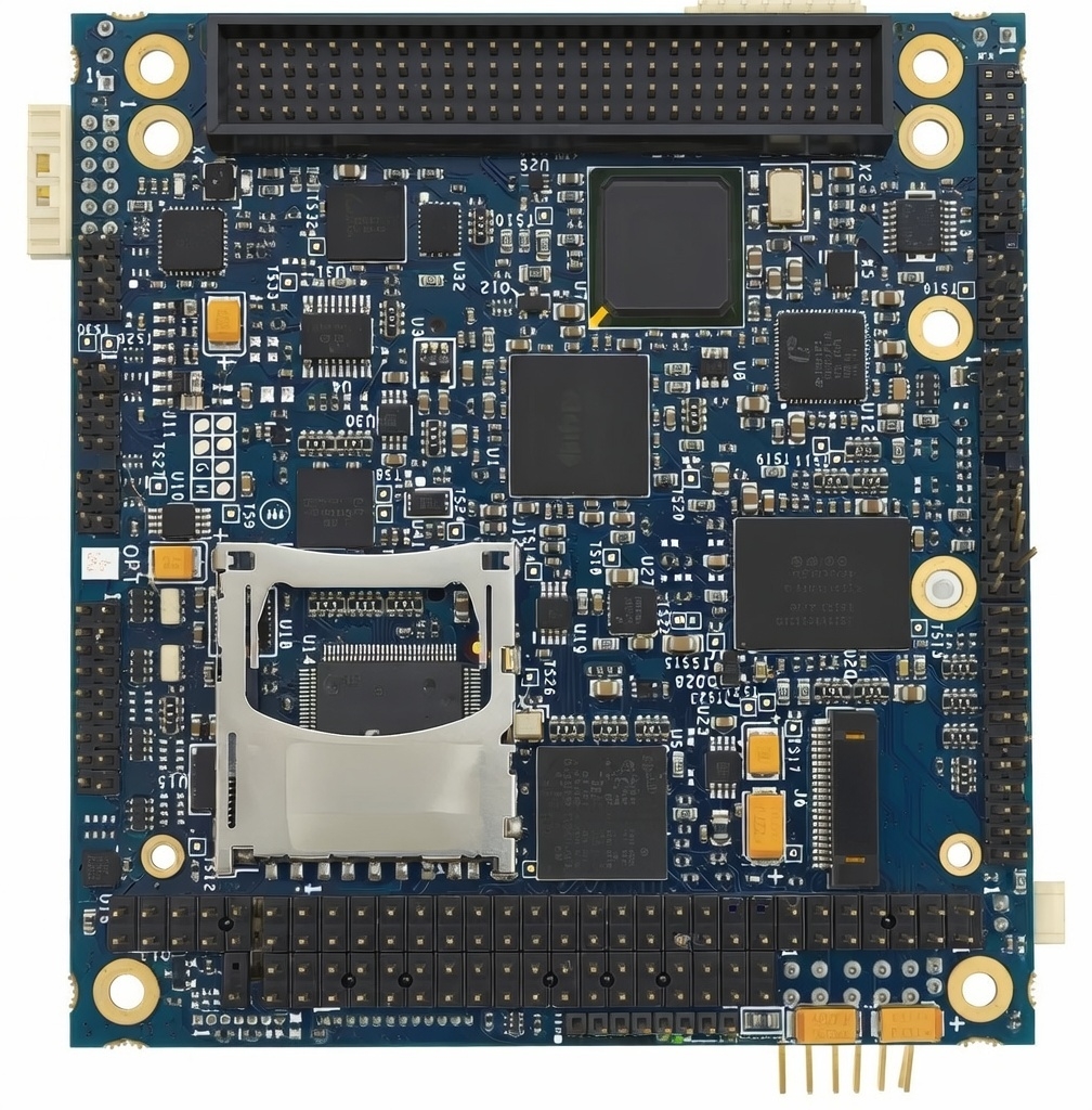
PCB
PCB Design Software
To begin, one must understand how to design a PCB. Circuit boards are created by engineers, innovators, or designers using specialized PCB design software—such as Altium Designer, OrCAD, PADS, KiCad, Eagle CAD, or EasyEDA. Once a PCB design has been reviewed, it is converted into Gerber files and sent to a manufacturer for production. To avoid errors that can occur when transferring files between different software programs, it is best to use widely adopted PCB design tools.
PCB Design Tips
1. Layout Planning
① Component Placement: Prioritize the placement of critical and large components, taking their heat dissipation requirements into account. Ensure sufficient space is left for components that require manual soldering.
② Signal Flow: Keep signal paths as short and direct as possible to minimize signal loss and interference.
③ Power and Ground Traces: Power and ground traces should be as wide as possible to reduce impedance and increase current-carrying capacity.
2. Layer Stack-up Design
① Multi-layer Boards: Select an appropriate multi-layer board configuration based on circuit complexity and signal frequency to achieve better signal isolation and power distribution.
② Ground Plane Allocation: Utilizing multiple ground planes can effectively reduce electromagnetic interference (EMI) and address electromagnetic compatibility (EMC) issues.
3. Routing Strategy
① Trace Width: Choose an appropriate trace width based on the amount of current the trace will carry to prevent overheating. ② Differential Pair Routing: For high-speed differential signals, ensure equal trace lengths and consistent spacing to minimize signal skew.
③ Avoid 90-Degree Angles: Use 45-degree angles or arc-shaped traces to reduce reflections in high-frequency signals.
4. Vias and Interconnections
① Minimize Vias: Reduce the number of unnecessary vias to lower manufacturing costs and improve signal integrity.
② Use of Blind and Buried Vias: Incorporate blind and buried vias in multi-layer PCB designs to increase routing flexibility and save board space.
5. Thermal Design
① Heat-Sensitive Components: Carefully position heat-sensitive components—keep them away from heat sources or provide dedicated heatsinks.
② Thermal Resistance Analysis: Use thermal simulation software to analyze thermal resistance and optimize the cooling design.
6. Design for Testability (DFT)
① Test Points: Include test points at critical nodes to facilitate testing during production and subsequent repairs.
② Boundary Scan: Implement boundary scan technology to enhance the testability of the circuit board.
General principles for PCB design include:
1. Determining Dimensions and Component Placement
Appropriate Dimensions: Excessive size can lead to increased impedance, poorer noise immunity, and higher costs; conversely, a board that is too small may hinder heat dissipation and increase susceptibility to interference.
High-Frequency Components: Keep connections as short as possible to minimize parasitic parameters and electromagnetic interference (EMI).
Interference Isolation: Separate components that are sensitive to interference; keep input and output components as far apart as possible.
High-Voltage Components: Increase spacing to prevent short circuits, and position them away from areas where they might be accidentally touched during debugging.
Heavy/Heat-Generating Components: Components weighing over 15g should be secured with brackets; large, heavy, or high-heat-generating components should be mounted on the chassis base rather than directly on the PCB. Keep heat-sensitive components away from heat sources.
Adjustable Components: Place internal adjustments in easily accessible locations; align external adjustments with the corresponding knobs or controls on the chassis panel.
Reserved Space: Allocate space for mounting holes and brackets to ensure structural stability during assembly.
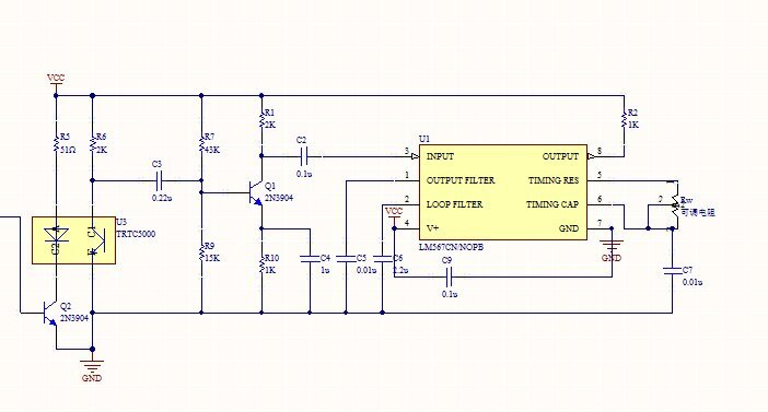
PCB schematic
2. Layout by Functional Unit
Align with Signal Flow: Arrange functional units according to the signal flow, ensuring a consistent direction to minimize signal loss and interference.
Center Core Components: Position the core component of each functional circuit at the center of its respective unit. Arrange components uniformly, neatly, and compactly to keep lead lengths short.
High-Frequency Circuit Layout: Account for distributed parameters; align components in parallel whenever possible (this enhances aesthetics, simplifies soldering, and facilitates mass production).
Board Edges and Shape: Maintain a distance of at least 2mm between components and the board edge. A rectangular board shape is preferred, with a recommended aspect ratio of 3:2 or 4:3. For boards exceeding 200x150mm, mechanical strength must be taken into consideration.
Excellent PCB design is the perfect combination of software tools, layout guidelines, and thermal/manufacturing considerations. Only by rationally planning dimensions and stack-ups, and following signal flow and isolation principles, can we reduce EMI interference and achieve highly reliable, mass-producible circuit boards. You may contact iPCB for professional PCB design services.