A Trustworthy PCB and Electronic Manufacturing Enterprise! Contact Us


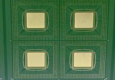
IC carrier board is the substrate used to package IC bare chips.
1. Carrying transistor IC chip.
2. There are circuits inside to conduct the connection between the chip and the circuit board.
3. Protect, fix, and support IC chips, provide heat dissipation channels, and are intermediate products that communicate between chips and PCBs.
The birth of IC carrier board
In the mid-1990s, its history was less than 20 years old. New integrated circuit ICs and high-density packaging forms represented by BGA ball grid array packaging, CSP chip size packaging, etc. have emerged, thus creating a necessary new carrier for packaging - IC packaging substrate.
The development history of transistors: electron tubes → transistors → through-hole mounting → surface packaging SMT, → wafer level packaging CSP, BGA, → system packaging (SIP)
Printed circuit boards and transistor technology are interdependent, close, penetrating, and closely coordinated. Only PCB can achieve electrical insulation and power connections between various chips and components, and provide the required power characteristics.

IC carrier board technical parameters
Number of layers: 2 to more than 10 layers
Plate thickness: usually 0.1~1.5mm
Minimum plate thickness tolerance: 0.05 micron
Minimum hole diameter: through hole 0.1mm, micro hole 0.03mm
Minimum line width/space: 10~80 microns
Minimum ring width: 50 microns
Shape tolerance: 0~50 microns
Required technology: buried blind vias, impedance, buried resistance and capacitance
Surface coating: Ni/Au, soft gold, hard gold, nickel/palladium/gold, etc.
Board size: single IC carrier board ≤240*90mm
IC carrier board require more precision, high density, high pin count, small volume, smaller holes, disks, and lines, and ultra-thin core layers. Therefore, it is necessary to have precise inter-layer alignment technology, line imaging technology, electroplating technology, drilling technology, and surface treatment technology. It has put forward higher requirements for product reliability, equipment and instruments, materials and production management in all aspects. Therefore, the technological threshold for IC carrier boards is high and research and development is difficult.
Compared with traditional PCB manufacturing, the technological difficulties of IC carrier boards need to be overcome:
1. Core board production technology: The core board is thin and easy to deform, especially when the board thickness is ≤0.2mm. Breakthroughs in process technology such as panel structure, board expansion and contraction, lamination parameters, and interlayer positioning system are needed to achieve ultra-thin Effective control of core board warpage and lamination thickness.
2. Microhole technology: equal window opening process, laser drilling micro-blind hole process, blind hole copper plating and hole filling process.
2.1 The conformal windowing process, Conformalmask, is a reasonable compensation for laser blind hole windowing. The diameter and position of the blind hole are directly defined through the opened copper window.
2.2 Things involved in laser drilling of micro holes: hole shape, upper and lower aperture ratio, side erosion, glass fiber protrusion, residual glue at the bottom of the hole, etc.
2.3 Blind hole copper plating involves: hole filling ability, blind hole voids, dents, copper plating reliability, etc.
At present, the diameter of micropores is 50~100 microns, and the number of stacked pore layers reaches 3, 4 and 5 levels.
3. Pattern formation and copper plating technology
3.1 Line compensation technology and control; Fine line production technology; Copper plating thickness uniformity control technology; Micro-etching control technology for fine lines.
3.2 The current line width and spacing requirements are 20~50 microns. The copper plating thickness uniformity requirement is 18 microns, and the etching uniformity is ≥90%.
4. Solder mask technology includes plug hole technology, solder mask printing technology, etc.
The surface height difference of the solder mask on the IC carrier board is less than 10 microns, and the surface height difference between the solder mask and the pad is no more than 15 microns.
5. Surface treatment technology
The uniformity of the thickness of nickel/gold plating; the process of plating both soft gold and hard gold on the same plate; the process technology of nickel/palladium/gold plating. Lineable surface coating, selective surface treatment technology.
6. Detection capabilities and product reliability testing technology
6.1 It is necessary to equip a batch of testing equipment/instruments that are different from traditional PCB factories.
6.2 Master reliability testing technology that is different from conventional ones.
7. Taken together, there are more than ten aspects of process technology involved in the production of IC carrier boards:
Graphics motion compensation
Pattern plating process for copper plating thickness uniformity
Full-process data expansion and contraction control
Surface treatment process, soft gold and hard gold selective plating, nickel/palladium/gold plating process technology
Core board sheet production
High reliability detection technology micro hole processing
If the 3rd, 4th and 5th order are stacked, the production process
Multiple lamination, lamination, lamination ≥ 4 times drilling ≥ 5 times plating ≥ 5 times.
Wire patterning and etching
High-precision alignment system
Solder mask plugging process, electroplating micro-hole filling process

IC carrier board classification
Distinguished by packaging form
1. BGA carrier board
BallGridAiry, its English abbreviation BGA, ball array package.
This type of packaged board has good heat dissipation and electrical performance, and can add a large number of chip pins, and is used in IC packages with a pin count of 300 or more.
2. CSP carrier board
CSP is the abbreviation of chipscale packaging, wafer level packaging.
It is a single-chip package that is lightweight and small. Its package size is almost the same or slightly larger than the size of the IC itself. It is used in memory products, communication products, and electronic products with a low pin count.
3. Flip chip carrier board
Its English name is FlipChipFC, which is a package form in which the front side of the chip is flipped over and directly connected to the carrier board with bumps.
This type of carrier board has the advantages of low signal interference, low connection circuit loss, good electrical performance, and efficient heat dissipation.
4. Multi-chip module
In English it is Multi-ChipMCM, and in Chinese it is called multi-core chip module. Put multiple chips with different functions into the same package.
This is the best solution for electronic products to become light, thin, short, smaller than high-speed and wireless. Used in high-end large computers or special performance electronic products.
Since there are multiple chips in the same package, there are currently no more complete solutions for signal interference, heat dissipation, thin circuit design, etc. This is a product that is under active development.
Classification by IC carrier board material
1. Hard board packaging carrier board
Rigid organic packaging substrate made of epoxy resin, BT resin, and ABF resin. Its output value accounts for the majority of IC packaging substrates. The CTE thermal expansion coefficient is 13~17ppm/℃.
2. Soft board packaging carrier board
The packaging substrate is a flexible base material made of PI polyimide, PE polyester, and resin, with a CTE of 13 to 27 ppm/℃.
3. Ceramic substrate
Packaging substrates made of ceramic materials such as aluminum oxide, aluminum nitride, and silicon carbide. CTE is very small, 6~8ppm/℃.
Differentiated by connected technology
1. Wire bonding the carrier board
Gold wires connect the IC to the carrier board.
2. TAB carrier board
TAB——TapeAutomatedBonding, tape and reel automatic binding and packaging production.
The internal pins of the chip are interconnected with the chip, and the external pins are connected with the packaging board.
3. Flip chip bonding carrier board
Filpchip flip-mounting, turn the front side of the chip over, and then directly connect it to the carrier board in the form of bumping.