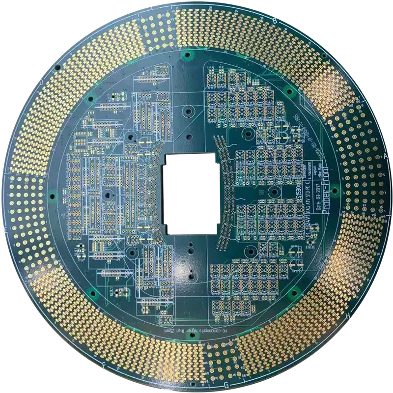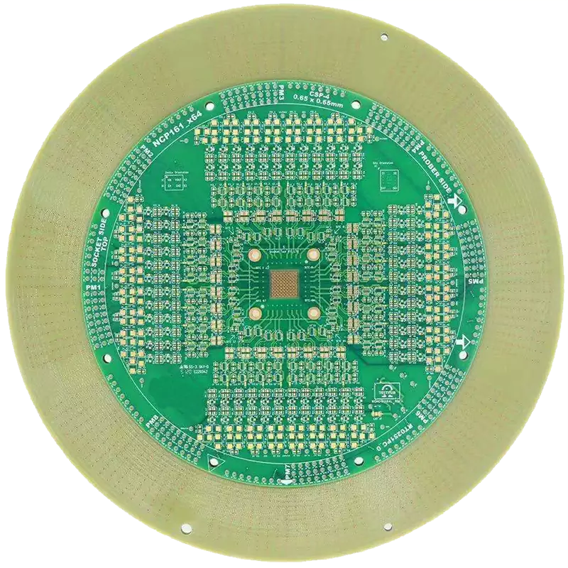

Product Name: IC Test Board
Layer: 46L
Material: 85N
Finished thickness: 6.0mm
Copper plating thickness: 1oz
Surface treatment: ENIG+gold plating
Minimum line width/spacing: 2.5mil/2.5mil
Minimum aperture: 0.1mm
Aperture ratio: 48:1
Product application: ATE, Semiconductor testing
With the rapid development of semiconductor integrated circuits, it has also driven the development of supporting industries such as integrated circuit packaging and testing. In the semiconductor integrated circuit testing industry, the demand for IC Test Board has gradually increased. Currently, this type of IC Test Board is still mainly composed of 10-60 layers, and high-end ones can reach up to 70 layers or more. iPCB has also followed suit and has made a large amount of technical reserves in the field of IC Test Board, which has been recognized by customers.
Characteristics of IC Test Board
1. The IC Test Board has a greater thickness
The IC Test Board has a high number of layers. In order to avoid problems such as board warping caused by thin boards and to ensure the flatness requirements of probe testing during use, the thickness of the IC Test Board is generally between 4.0mm and 6.0mm. When making IC Test Boards, such thick boards have high equipment capabilities and basic protection measures need to be taken for the board.
2. IC Test Board requires high aperture ratio
The design of IC Test Board is relatively thick. In order to have more functions, the design is generally compact, and the aperture design is relatively small, resulting in high aperture of the board. This also increases the difficulty of circuit board production. For such boards, especially the electroplating process, special control is required, such as choosing pulse electroplating and other processes to ensure.
3. The installation and positioning of NPTH holes require high aperture requirements
The conventional NPTH hole diameter tolerance in the circuit board industry is generally controlled within+/-0.05mm. In semiconductor testing, due to the contact between the probe and the solder pad, this type of board has extremely high requirements for the installation and positioning of NPTH hole diameter. The NPTH hole diameter tolerance may be controlled within+/-0.025mm, and in some cases, it is strictly controlled within+/-0.015mm. For PCB manufacturing, it is undoubtedly a great challenge, requiring special control over the diameter of the drilling bit and the status of the drilling rig, such as customizing drill bits with special diameter tolerances and precision correction of the drilling rig before drilling.
4. High requirements for contact pad hardness and flatness
Solder pads are mainly used for long-term continuous contact testing, and the hardness and flatness requirements of solder pads are extremely high. The industry generally uses local electroplating to produce solder pads, increasing the hardness of solder pads to meet the needs of frequent long-term contact of products. For the balance of solder pads and the manufacturing of circuit boards, there are certain requirements for the selection of equipment such as grinding plates in each process. The selection of equipment has a great impact on the flatness of solder pads.
5. IC Test Board has stricter requirements for warpage
The conventional board warping requirement in the circuit board industry is generally controlled at 0.75%. In the field of semiconductor testing, due to the strict requirements for testing semiconductor wafers and other products, the overall board warping of the board is strictly controlled at 0.5%. For stricter requirements, it may be required to control at 0.3%. Some products also require a board warping of 0.1%. New requirements have been put forward for circuit board production, and more attention should be paid to details in control to ensure quality and meet customer needs.
IPCB focuses on customized services for the circuit board industry, with a maximum processing layer of 110 layers. Its products cover various types such as multi-layer PCB, POFV, copper paste plug hole, high speed PCB, rigid-flex PCB, HDI PCB, local inlay (copper block, special material), thick copper plate, PTFE PCB, local electroplating, mixed surface treatment, back drilling, steps, backboards, IC Test Board, etc. The products are widely used in communication, industrial control automation, power and new energy, automotive electronics, medical equipment, rail transit, aviation and military industries, serving more than 8000 customers worldwide.
Product Name: IC Test Board
Layer: 46L
Material: 85N
Finished thickness: 6.0mm
Copper plating thickness: 1oz
Surface treatment: ENIG+gold plating
Minimum line width/spacing: 2.5mil/2.5mil
Minimum aperture: 0.1mm
Aperture ratio: 48:1
Product application: ATE, Semiconductor testing
iPCB Circuit provides support for PCB design, PCB technology, and PCBA assembly. You can request technical consultation or quotation for PCB and PCBA here, please contact email: sales@ipcb.com
We will respond very quickly.