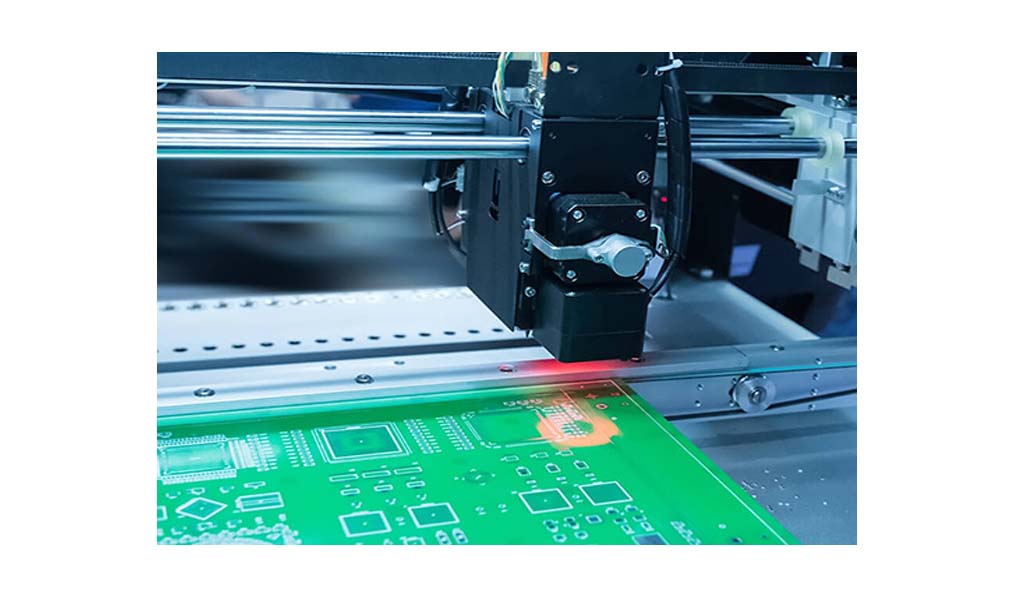
PCB board is one of the most basic components in electronic equipment manufacturing. It is composed of a variety of different materials and plays different roles in different devices. Among them, multilayer PCB board has attracted more and more manufacturers' attention due to its complex structure and difficulty in production. So what is multilayer pcb fabrication process?

The following is a detailed description of the multilayer printed circuit board manufacturing process:
Cutting: PCB board factory does not directly manufacture copper clad laminates, prepregs, copper foils and other substrates, but purchases the required substrates from substrate manufacturers upstream of the industrial chain. The substrates are all standard large sizes when they leave the factory, such as 1mx1m (or 1mx1.2 m). Then before PCB manufacturing, it needs to be cut into the size required for the production line according to the specifications of its own processing equipment.
After cutting, for the multilayer pcb fabrication process, the inner layer circuit is first made, such as inner layer pattern making, lamination and other processes, and then the process returns to the same process as the double-layer board, such as drilling, electroplating, outer layer pattern making, etc., and finally various tests and packaging and delivery.
Inner layer pattern making: The inner layer of the multi-layer board usually uses a thin double-sided copper-clad substrate. After the inner layer circuit is formed on its surface, it is pressed to obtain a multi-layer board.
A photosensitive dry film is pasted on the inner double-sided copper-clad board, and then a film of the inner layer circuit is pasted and exposed. After exposure, it is developed, and then etched with an etching machine to remove unnecessary copper foil.
After etching, the inner layer circuit has appeared. At this time, it is necessary to remove the protective film that protects the circuit from being etched. This is the film removal process.
Next is the inspection of the inner layer, which is carried out by automatic optical inspection (AOI). Before lamination, in order to improve the bonding ability of the copper foil and the prepreg, browning treatment is required.
Browning treatment: In order to improve the bonding strength between copper foil and resin, browning treatment is carried out to increase the contact area between copper foil and resin, increase wettability, and prevent water from being generated under high temperature and high pressure and causing the board to explode.
Lamination: The prepared inner layer board, prepreg and outer copper foil are stacked in sequence and formed into a whole by hot pressing. This step is to ensure the bonding strength between the layers and the stability of the structure.
Drilling: After lamination, drilling is carried out to produce through holes between the layers of the circuit board to achieve the purpose of connecting the layers.
Electroplating and solder mask: The holes are electroplated to ensure conductivity; solder mask is applied by screen printing ink, and the parts to be soldered are exposed through exposure and development after pre-baking, and the other parts are covered with solder mask to prevent short circuits.
Surface treatment: The surface of the PCB board is treated, such as spray painting, immersion gold, etc., to prevent the board from moisture and oxidation.
Forming and cutting: The PCB is cut into the required dimensions and formed.
Testing and packaging: Electrical performance is checked by non-automatic or fully automatic testing machines, and vacuum-sealed packaging is carried out for shipment after meeting customer requirements.
Circuit board manufacturing is actually a complex and delicate process, and every link requires strict control and management. With the development of science and technology, multilayer pcb fabrication process is also constantly innovating and improving to meet the needs of continuous upgrading of electronic products.
We believe that in the future, multilayer pcb fabrication process will develop in the direction of higher precision, higher efficiency, and more environmental protection, providing strong support for the development of the electronics industry.