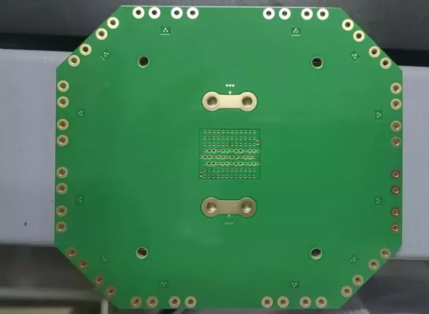
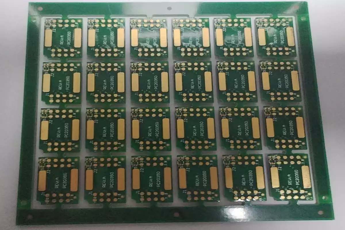
PCB Via, also known as through-hole, through hole. It opens from the top to the bottom end of the circuit. For example, in a double-layer PCB, Via vias penetrate through layers 1 and 2, and in a four layer PCB, Via vias penetrate through layers 1, 2, 3, and 4.
There are mainly two types of PCB via hole: PTH and NPTH
1. Plated Through Hole (PTH) with copper walls, typically consisting of current through hole (VIA PAD) and component hole (DIP PAD).
2. Non Plating Through Hole (NPTH), with no copper on the hole wall, usually has positioning hole and screw hole.
PCB Blind Via: PCB blind hole can only be seen from the top or bottom layer. The additional layers are invisible. That is to say, blind hole are drilled out from the outside, rather than penetrating the entire layer.
PCB blind vias can grow up to 1 to 2 or 4 to 3 (benefit: 1 and 2 conductivity will not affect 3 and 4 wiring); The through-hole penetrates through layers 1, 2, 3, and 4. Layer wiring has an impact. But blind hole are expensive and require the use of laser drilling machines. Blind hole board is used to connect the outer surface layer and one or more inner layers. One side of the hole is on the side of the wrench, and then it leads to the inside of the wrench to cut off; Simply put, the outer surface of a blind hole can only be seen on one side, with the other side inside the wrench. Generally used for PCB board with four or more layers.
PCB Buried Via: PCB buried hole refer to internal via hole. After pressing, it cannot be seen, so it does not occupy the size of the outer plane or object surface. The upper and lower sides of the hole are both inside the inner layer of the wrench, that is, buried inside the wrench. Simply put, it is sandwiched in the middle of the waist. We cannot see these processes from the outside, nor can we see the top and bottom layers. The advantage of making buried hole is to increase wiring space. However, the cost of the buried hole manufacturing process is high, and ordinary electronic products are not suitable for use, only applied to particularly high-end products. Generally used for PCB with six or more layers.

PCB
PCB VIA is usually R outer diameter - r inner diameter>=8mil (0.2mm), which is the minimum aperture for mechanical drilling; If it is a blind hole or buried hole, the minimum aperture is 4mil (0.1mm), and laser is required for this type of hole. The smaller the hole, the more expensive it is. It is recommended to use 10/18mil and 12/20mil hole for through-hole, and 16/24mil hole can be used for power hole.
There is no absolute standard for PCB design. For high current applications, the outer diameter of the via can be made larger and the inner hole can be made smaller. But PCB manufacturing companies generally recommend using a 0.5MM inner diameter because using a 0.5mm drill pin is not easy to break. Drill needles below 0.5MM are prone to breakage.
After reading this experience, I still feel that it is not intuitive enough. If you think about it, just go to the previous photo! Positive and negative films: For a four layer board, the first thing to understand is the difference between positive and negative films, that is, the difference between layers and planes. The positive film is a commonly used routing method for the top layer and strata, with copper wires at the routing points, supplemented by large copper wires from Polygon Pour. Negative film is exactly the opposite. Copper is the default for wiring and branching, which generates negative film. Afterwards, the entire layer was coated with copper. What needs to be done is to separate the copper and set separate coatings. Copper mesh. In previous versions of PROTEL, Split was used for partitioning, but in the current version of Altium Designer, Line and agile key PL are directly used for partitioning. The dividing line is not suitable for being too thin, I used 30mil (about 0.762mm). When dividing copper wires, simply draw a closed polygon box with LINE and double-click the copper wire to set the network. Both positive and negative films can be used for internal electrical layers, and positive films can also be successfully implemented after wiring and copper plating. The advantage of negative film is that it defaults to increasing large copper deposition, eliminating the need for reconstruction when adding vias, changing copper deposition volume, etc., saving time in calculating new copper deposition. The middle waist half layer is used for the power layer and geological layers, with most of it being a composite copper layer.
The advantages of using blind hole and buried hole are considered appropriate. In non through-hole technology, the application of blind hole and buried hole can greatly reduce the size and quality of HDI PCB, reduce the number of layers, increase electromagnetic compatibility, and enhance the unique style of electronic products, reducing costs. At the same time, it also makes default office easier and more convenient. In traditional PCB pre-processing, through hole can cause many problems. Firstly, they occupy a significant amount of pipeline space. A densely packed through-hole also poses a significant obstacle to the inner layers of multi-layer PCB. These through hole occupy the space required for wiring and are densely distributed. The penetration of current through the source surface and ground plane can also damage the special impedance of the power source ground plane, causing the power source ground plane to fail. The common sense mechanical drilling method will be 20 times the workload of an office that is considered appropriate and uses non through-hole technology. In PCB pre setting, although the size of solder pads and vias has gradually decreased, if the thickness of the board layer is disproportionately reduced, the aspect ratio of the through hole will increase, and the increase in the aspect ratio of the through hole will reduce reliability.
With the maturity of advanced laser drilling technology and plasma dry etching technology, the application of non through small blind hole and small buried hole has become possible. If the diameter of these non through hole is 0.3mm, the parasitic parameter variables generated are about 1/10 of the initial common sense hole, increasing the reliability of the PCB. Because it is considered appropriate to use non via technology, there will not be large via hole on the PCB, which can provide more wiring space. The remaining space can be used as a shielding field for large planes or object surfaces to improve EMI/RFI performance. At the same time, more remaining space can also be used for inner shielding components and critical network cables to achieve optimal electrical performance. The use of appropriate non through hole can facilitate the fan out of component pins. High density pin components (such as BGA packaging components) are easy to wire, reduce string length, and meet the timing requirements of high-speed PCB.
The disadvantages of using blind hole and buried hole that are deemed appropriate are: the main disadvantages are the high cost and complex processing of HDI board. This not only increases costs, but also increases processing risks. The special circumstances of testing and measurement are difficult to adjust, as this recommendation minimizes the need for blind hole and buried hole. The problem is that the size of the wrench is limited, and it can be used in situations of helplessness.
PCB Via is the most common type, as long as you hold the PCB up and face it towards the light, you can see that the hole with bright light are via hole. This is also the simplest type of hole, because during production, only a drill or laser is needed to directly drill the entire circuit board, and the cost is relatively cheap.

PCB
Mechanical characteristics of PCB Via through hole
1. PCB Via through-hole diameter: The diameter of PCB Via must exceed the diameter of the plug pins and leave a certain margin. The minimum diameter that can be achieved by threading through hole is limited by drilling and electroplating technology. The smaller the diameter of the through-hole, the smaller the space occupied by the circuit board, the smaller the parasitic capacitance, and the better the high-frequency performance, but the cost will also be higher.
2. Via through-hole solder pad: The solder pad realizes the electrical connection between the plated inner layer of the through-hole and the surface (or interior) of the printed circuit board.
3. The capacitance of PCB via: Each via has a parasitic capacitance to ground, which can slow down or degrade the rising edge of digital signals, which is not conducive to the transmission of high-frequency signals. This is the main adverse effect of via parasitic capacitance. In general, the impact of through-hole parasitic capacitance is minimal and can be ignored. The smaller the diameter of the through-hole, the smaller the parasitic capacitance.
4. Inductance of PCB Via: Each Via through-hole has parasitic series inductance, which reduces the effectiveness of the power supply bypass capacitor and deteriorates the overall power supply filtering effect. For digital circuits, the parasitic inductance of Via vias has a greater impact than parasitic capacitance, so it is advisable to avoid using Via vias for high-frequency circuits as much as possible.