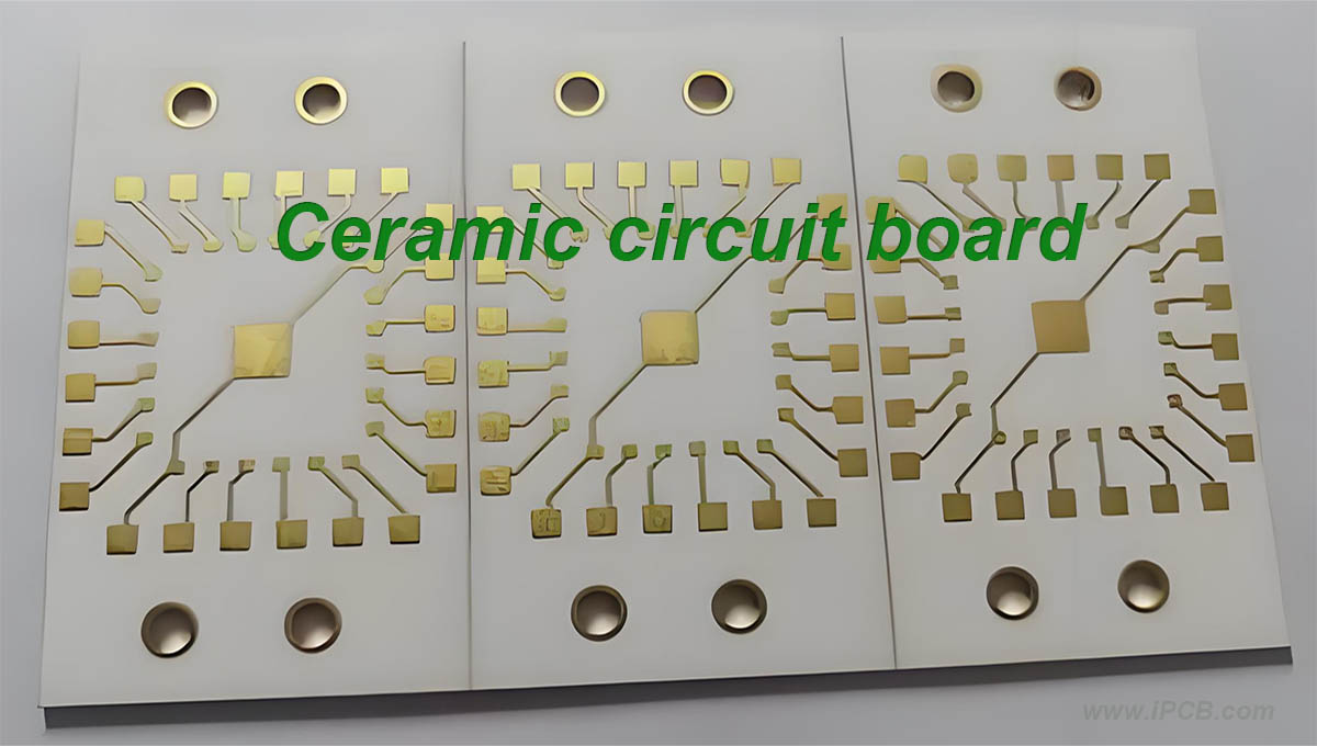
With the development of material technology, ceramic circuit boards have been increasingly used in scientific research and industrial applications due to their superior physical and chemical properties. Whether it is precision microelectronics, heavy industries such as aviation and shipbuilding, or daily necessities for ordinary people, ceramic circuit boards can be found in almost all fields.
However, ceramic circuit boardshave a dense structure and are somewhat brittle. Although they can be manufactured by ordinary mechanical milling cutters, there are stresses during the manufacturing process, especially for some very thin ceramic sheets, which are very easy to break. This makes the manufacture of ceramic circuit boards a difficult point for widespread application.
As a flexible manufacturing method, lasers have demonstrated extraordinary capabilities in the manufacturing process of ceramic circuit boards. The following is an explanation of laser cutting and drilling of ceramic circuit boards.

Ceramic circuit boards
Laser drilling of ceramic circuit boards
In the microelectronics industry, traditional processes use PCB as the circuit substrate. However, with the development of the industry, more and more customers require their microelectronic products to have more stable performance, including the stability of mechanical structures, the insulation performance of circuits, and so on. Therefore, ceramic materials have received more and more applications. The current mainstream ceramic materials are ceramic alumina and ceramic aluminum nitride, and the mainstream thickness of ceramic materials is less than 2mm.
In order to achieve more complex circuit design, customers generally require double-sided circuit design, and form upper and lower conduction by pouring silver paste or sputtering metal through the through hole. At the same time, in order to meet the needs of external packaging, the appearance of circuit components also has various changes, including some rounded corners or other anomalies. For such product design, mechanical manufacturing methods are very difficult. Even if it can be manufactured, its yield rate is very low. The widely cited chemical etching method or electric spark manufacturing method for metal manufacturing cannot be applied due to the superior physical and chemical properties of ceramics. In this regard, laser non-contact manufacturing can greatly improve the feasibility and yield of ceramic laser manufacturing.
Laser cutting of ceramic circuit boards
For samples of 0.635mm thick alumina and 0.8mm thick ceramic aluminum nitride special-shaped cutting. It can be seen that not only the cutting edge is smooth and there is no edge collapse, but the thermal impact of the cutting edge can be effectively controlled. Even if the ceramic has been metallized, it can still be accurately cut without damaging the metallized part.
Laser linear scribing manufacturing of ceramics has appeared in the United States a long time ago. However, it can be seen that today's laser cutting technology for ceramic circuit boards has been far-reachingly developed.
Traditional CO2 high-power laser is the traditional process in the current application of ceramic straight-line cutting. Due to its efficient cutting and basically flat cutting section, it is currently the mainstream process for ceramic sub-board manufacturing. However, for some higher-demand ceramic cutting manufacturing, such as straight-line cutting of circuit unit shapes, it is not applicable. Under an 80x microscope, we can see that the ceramic circuit board cut by high-power CO2 laser has stamp-like bumps on the edge, with a fluctuation range of about 50~90um.
How can we ensure the high efficiency of laser cutting of ceramic circuit boards, while reducing stamp-like edges and improving manufacturing effects? Our company has developed a new solution. With our current ceramic circuit board manufacturing capabilities, we can cooperate with customer needs to carry out laser half-cutting or laser full-cutting processes for ceramic circuit boards, and meet customer requirements for accuracy, effect and manufacturing efficiency.