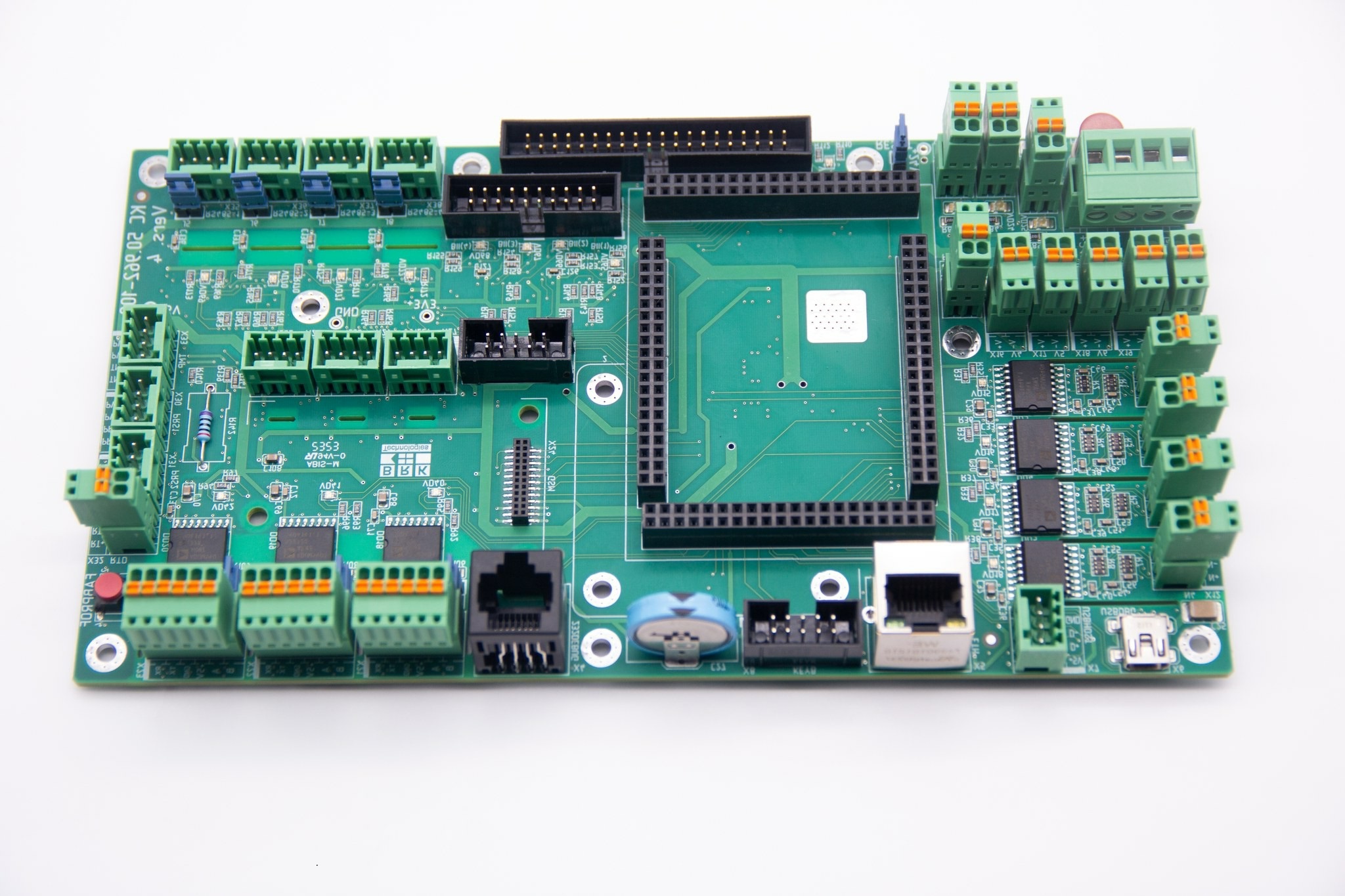
The main PCB board is the carrier of the electrical interconnection of electronic components, known as the “mother of electronic products.” PCB's main function is to make a variety of electronic components form a predetermined circuit connection and play the role of relay transmission. It is formed on a universal substrate according to the predetermined design for point-to-point connections and printed components.
The electronic components on the PCB board are resistors, capacitors, diodes, transistors, MOSFETs, LEDs, integrated chips, and so on. Different electronic components play various roles in the circuit.
Main PCB board fabrication process:
(1) Inner layer production: produce the inner layer of PCB board lines.
(2) Internal inspection: testing and repairing the board lines.
(3) Press-fit: press several inner layers into one board.
(4) Drilling: according to customer requirements, using a drilling machine to drill the board with different diameters and sizes of holes, so that the board can pass through the holes and then follow up the processing of plug-ins, but also to help the board with heat dissipation.
(5) Copper: the outer layer of the board has been drilled holes in copper plating so that the board of all layers of lines of conduction.
(6) Outer layer: the outer layer with the first step of the inner layer of the process is more or less the same, its purpose is to facilitate the subsequent process to make the line.
(7) Secondary copper and etching: secondary copper plating, etching.
(8) Solder mask: can protect the board to prevent oxidation and other phenomena. Printing text to facilitate the subsequent welding process.
(10) Surface treatment: the side of the bare copper plate to be soldered is coated to form an organic skin film to prevent rust and oxidation.
(11) Molding: going out the board appearance required by the customer to facilitate the customer to carry out SMT mounting and assembly.
(12) Flying probe test: Test the board circuit to avoid short circuits that can cause board overflow.
(13) FQC: Final inspection, after completing all the processes, we will carry out sampling and full inspection.
(14) Packing and shipping: Vacuum pack the PCB boards, and pack them to ship for complete delivery.

Main PCB board and daughter PCB board connection collaboration can be realized through the welding mode, plug connection mode, and buried hole connection mode.
(1) PCB wire welding: this way does not need any connector, as long as the wire will be welded to the PCB printed board on the external connection point, and then the board outside the components or other parts can be welded directly. For example, the speaker in the radio, battery box, etc.
(2) PCB line welding: between two PCB printed circuit boards using line connection, both reliable and not easy to connect in error, and the relative position of the two PCB printed circuit boards is not restricted.
(3) PCB direct welding: direct welding between the printed circuit boards, this method is commonly used between two printed circuit boards for a 90-degree angle connection. It connects to become a whole PCB printed circuit board component.
PCB rigid and flexible boards can be connected by a connector snap-in or hotbar. Pre-positioned solder on the PCB pads, through the hot pressure melting solder, makes the FPC pads and PCB pads connected, which can effectively reduce the overall thickness of the PCBA, reserving a larger space for other components.
In the electronic product manufacturing industry, the connection and control between the main PCB board and daughter PCB board plays a key role in realizing the electrical function of electronic products, and the key to controlling the daughter board is to ensure the quality and stability of signal transmission between the main board and daughter board.This can be effectively realized through impedance control, reasonable layout and wiring, and selection of appropriate connection methods.