Copper foil is used in all circuit substrates, and in high-reliability applications, choosing the right copper-clad substrate can provide the best performance for the circuit.
There are many different types of copper foils, such as differences in weight (thickness) and characteristics between different copper foils. Understanding these differences can help engineers choose the right type of copper foil for different applications.
Electrolytic Copper Clad Manufacturing Technology
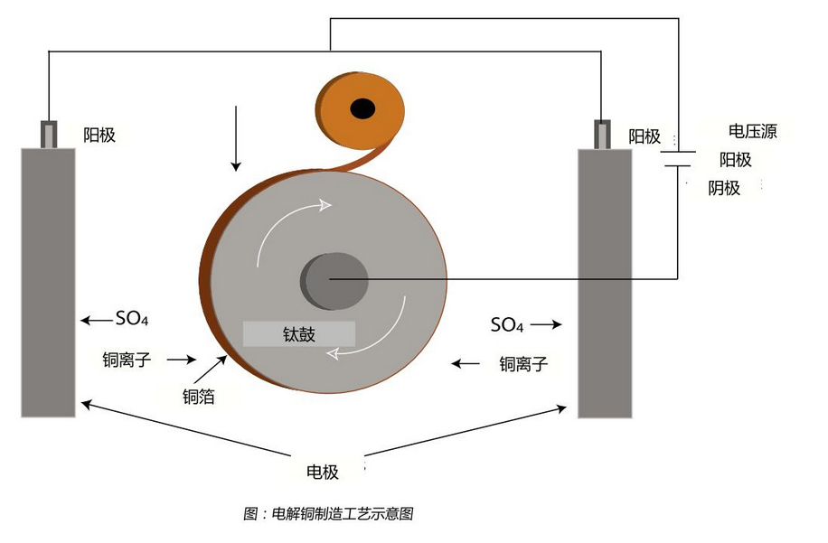
In electrolytic copper foil manufacturing technology, copper foil is formed by depositing copper ions from a chemical solution onto a rotating titanium drum. The titanium drum is connected to a DC voltage source where the cathode of the power source is connected to the titanium drum and the anode is immersed in a copper electrolyte solution. When the voltage is applied, the titanium drum rotates at a very slow諫, and the copper ions in the copper solution are slowly deposited onto the cathode surface of the titanium drum under the traction of the electric current. The inner copper surface of the titanium drum is relatively smooth, while the other side of the copper surface is relatively rough. The slower the titanium drum rotates, the thicker the copper deposits, and vice versa. The smooth and rough sides of the copper foil are processed in different ways to make them suitable for use in printed circuit boards. Processing copper foils enhances the bonding between the copper and the dielectric material. Another advantage is that the oxidation of the copper is slowed down to prevent discolouration.
Copper Foil Manufacturing Technology - Rolled Copper Foil
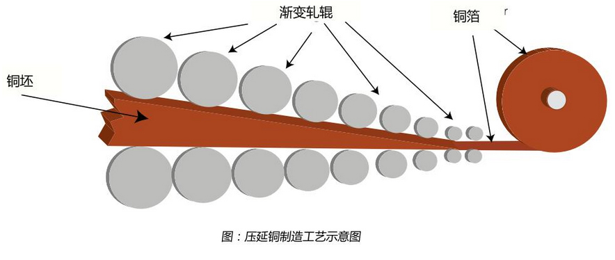
Copper Foil Manufacturing Technology - Rolled Copper Foil Rolled copper foil is produced by successive cold rolling operations. Starting from a pure copper billet, it is rolled continuously to reduce its thickness and extend its length. The smoothness of the surface depends on the condition of the rolling mill.
Copper foil resistors are coated with a metal or alloy on the rough side of the electrolytic copper foil to act as a resistive layer. The layer is then roughened with nickel particles. Reversed Copper Cladding and Lo Pro Copper Cladding Reversed Copper Cladding is a process whereby the smooth side of the electrolytic copper foil is treated. The process consists of applying a thin layer of treatment to the surface of the strain to roughen the surface of the strain. The purpose of this treatment is to improve the bonding between the copper foil and the dielectric and to increase the corrosion resistance of the copper foil. When combined with dielectric materials and laminated into multilayer boards, the treated surface of the copper foil is laminated onto the dielectric material. The treated copper surface is still relatively smooth, while the rough surface is still very rough. This is an advantage over standard electrolytic copper in that the rough surface of the outer layer does not require any further mechanical or chemical treatment before the circuitry is processed and the film is pressed dry. The roughness of the outer layer is sufficient to ensure the adhesion of the dry film. In the case of the Loro foil, a thin layer of adhesive is added to the treated surface of the reversed copper foil, creating a solid layer with enhanced adhesion. As with the reversed copper foil, the adhesive-treated side is pressed against the dielectric layer for a better bond. Rogers' R○4000 series data is a line of multilayer boards using Loro Copper.
Copper Clad Resistors
A metal or alloy is coated on the rough side of electrolytic copper foil to act as a resistive layer. The resistive layer can then be roughened with nickel particles.
Reversed Copper Clad and Lo Pro Copper Clad
Reversed copper foil is a process where the smooth side of electrolytic copper is treated. The process is to rough up the surface of the strain by applying a thin layer of treatment to the surface of the strain. The purpose of this treatment is to improve the bonding between the copper foil and the dielectric and to increase the corrosion resistance of the copper foil. When combined with dielectric materials and laminated into multilayer boards, the treated surface of the copper foil is laminated onto the dielectric material. The treated copper surface is still relatively smooth, while the rough surface is still very rough. This is an advantage over standard electrolytic copper in that the rough surface of the outer layer does not require any further mechanical or chemical treatment before the circuitry is processed and the film is pressed dry. The roughness of the outer layer is sufficient to ensure the adhesion of the dry film.
In the case of the Loro foil, a thin layer of adhesive is added to the treated surface of the reversed copper foil, creating a solid layer with enhanced adhesion. As with the reversed copper foil, the adhesive-treated side is pressed against the dielectric layer for a better bond. Rogers' R○4000 series data is a circuit multilayer board using Loro Copper.
The crystalline structure of electrolytic copper is based on the fact that the particles of the electrolytic copper are used in the longitudinal growth of the Z-axis of the copper foil. Typically, the cross-section of electrolytic copper has a sharp-piled fence appearance and a long (perpendicular) edge perpendicular to the plane of the copper. The water in the calendered copper is destroyed during the rolling operation of the copper blocks. The brinks are smaller than those of electrolytic copper, have an irregular spherical shape and are almost parallel to the surface of the copper foil.
Measurement of copper foil roughness
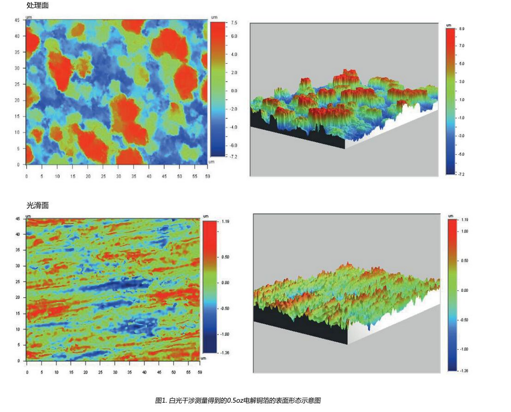
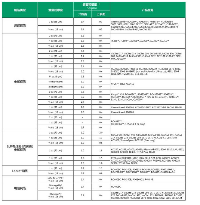
The surface roughness of copper foil can be measured mechanically or optically. Many references in the literature refer to the ‘Rz’ (peak to valley) value because it is measured by mechanical pipework gauges. However, in our experience, the Sq (RMS) roughness of the copper foil surface measured by non-contact white light interferometry is more consistent with actual conductor loss. Figure 1 shows the surface characteristics of 0.5oz electrolytic copper foil used on Rogers PTFE and TMM multilayer boards measured using non-contact white light interferometry. Table 1 shows the type of copper foil used on the Rogers lamination data and typical roughness information. A recent study (Ref. 7) has shown that the ‘upper surface’ roughness has a completely different structure than the dielectric surface and that it has virtually no effect on conductor loss in the transmission line.
The table below shows the roughness data of electrolytic and calendered copper foils of different thicknesses using an optical measuring instrument. The table also mentions which type of copper foil is used for which type of multilayer board at Rogers. It can be seen that calendered copper is the smoothest copper foil.
Electrical Performance of High Frequency Multilayer Circuit Boards
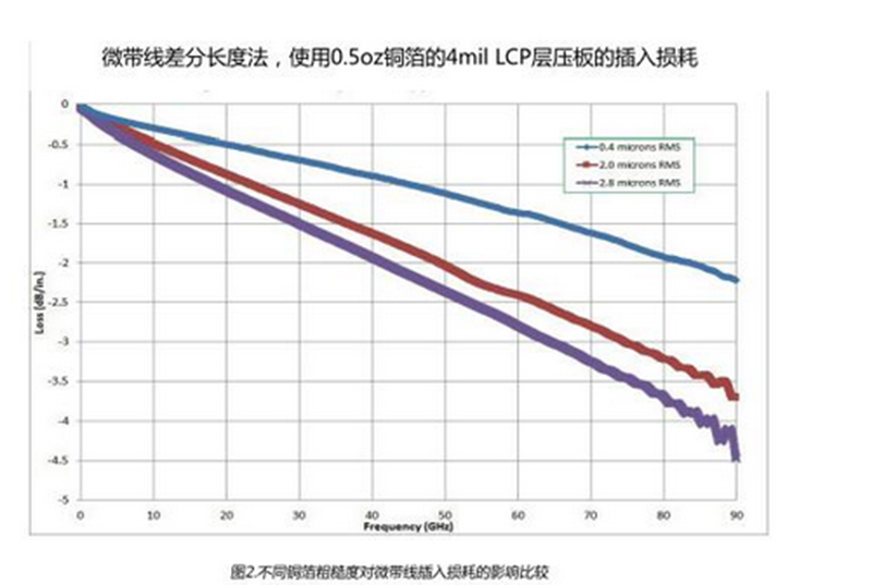
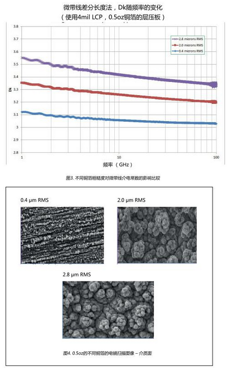
In waveguides, the surface roughness of the conductor has a significant effect on the conductor loss, which has been known since the early days of microwave engineering. In 1949, S.P. Morgan (Ref. 1) published numerical simulations showing that conductor surface roughness could lead to an exponential increase in conductor loss. Hammerstad and Jensen (Ref. 2) combined Morgan's model and data with a microstrip design methodology. The H αυ model became a ‘textbook’ (Ref. 3) method for calculating the effect of surface roughness on conductor losses. As higher frequencies and thinner multilayers are used, it has been found that the H α model significantly underestimates the effect of surface roughness on conductor loss (Refs. 5, 6). The ‘Hal-Huray’ model (Ref. 4), which is a development of the ‘first-principles’ analysis, has recently been adopted by commercial analogue design software. design software. In our experience, the ‘Ha‖l-Huray model can more accurately predict conductor losses over a range of multilayer board thicknesses and frequencies by appropriately tuning the input parameters. The ‘Hal-Huray’ model has been incorporated into Rogers' impedance and loss MwM software. We are currently working on developing the best possible ‘HalHuray’ input parameters for analogising the performance of Rogers' multilayer boards. Please check the Rogers Tap Centre on the Rogers website or contact a Rogers sales engineer in your area for the latest information. Rogers' research on copper foils (references 5, 6, 7) has also shown that copper foil roughness affects propagation constants, with rougher surfaces resulting in a significant increase in the effective dielectric constant. Fig. 3 shows the dielectric constant of a 50 ohm transmission line on a 4 mi liquid crystal polymer multilayer board (LCP) using copper foils with Sq values ranging from 0.4um to 28um. It can be seen that the Dk increases by nearly 10‰% for the circuit with the copper foil with the highest roughness. The effect of Cu foil roughness on phase response is not considered in the ‘Hall-huray’ model. The effect of Cu foil surface roughness on insertion loss is very obvious (Fig. 2). At 90 GHz, the insertion loss of a 50 ohm transmission line made of a 4-mi thick liquid crystal polymer (LCP) multilayer sheet, with a diecast copper foil (blue wire), is 汋2.2 dB/i η ch, which is almost identical to the model of a completely smooth copper perovskite conductor. Using a standard electrolytic copper foil on the same substrate with an Sq value of 2.oum, the insertion loss increases to 3.7 dB/inch. Fig. 4 shows the morphology of the surface roughness of the copper foil for the conductor with the data shown in Fig.2.
Mechanical Performance of Multilayers A. Thermal Shock Resistance Under certain extreme conditions of rapid thermal cycling, electrolytic copper foils may exhibit thermal stress cracks in narrower conductors. However, under the same conditions, the crack resistance of rolled copper is significantly improved. Although electrolytic copper foils have greater tensile strength and ductility, calendered copper foils have better elastic ductility before reaching permanent deformation. B. Copper Foil Bonding Force Since the bonding of resin to metal is mainly by mechanical bonding, the bonding force of copper foils in multilayer boards is directly related to the surface roughness of the treated copper foils. C. Bonding of strip line structures (PTFE substrates) SEM photographs show the differences in morphology and roughness between different copper foil types and the dielectric surface of the etched copper foil. If the circuit boards are bonded, sodium or plasma treatment of the dielectric surface is not necessary for electrolytic copper platens, provided that care is taken to protect the surface. However, for calendered copper circuit boards, where the smaller surface roughness of the copper foil will result in poorer mechanical bonding, antique textiles are necessary for reliable bonded assemblies. The different manufacturing methods of the two different types of copper foils in the Appendix result in differences in electrical and mechanical performance. The main differences are listed in Table 2.

Above is the introduction of copper foil for sharing circuit board materials, note that electrolytic copper foil and calendered copper foil have different properties.