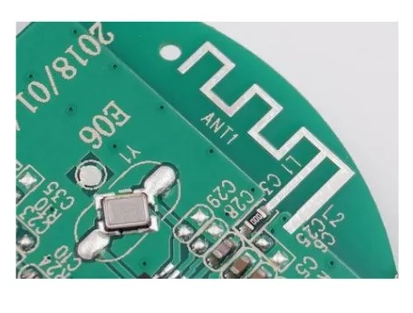
What is pcb antenna design?
It is an antenna placed on a printed circuit board. It uses traces as its conductive element. In other words, it forms a part of the circuit board as opposed to an external connection.
When used with RF circuits, it helps turn radio waves into small current pulses. It can also act as a transmitter and perform the opposite purpose.
Fabrication directly on the circuit board has several advantages, including lower cost and ease of integration. It is useful in electronic devices with wireless communications in various frequency bands, including cellular, Wi-Fi, and Bluetooth.
Working Principle of pcb antenna design
PCB printed antenna helps transmit or receive high-frequency electromagnetic waves. It works with high-frequency circuits to convert the energy of RF waves into electrical signals and vice versa. Here is its operation in more detail:
Transmission: RF circuits send varying charges to the antenna. The charges generate electromagnetic waves that radiate into space, carrying the transmitted signal.
Reception: The electromagnetic field induces charges in the antenna, generating fluctuating currents and voltages. The RF circuit decodes it to separate or extract the transmitted signal.
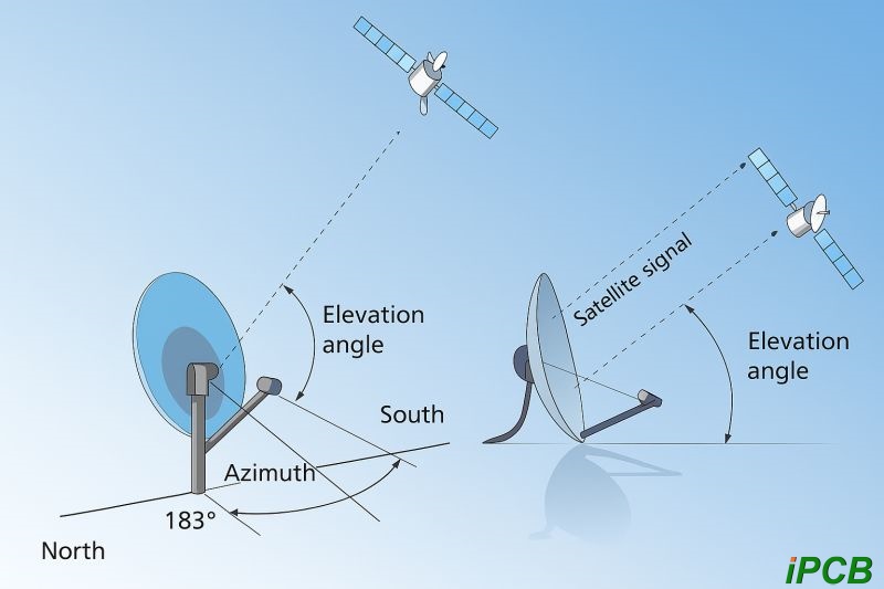
Wave radiation varies depending on its design. It is usually directional, semi-directional or omnidirectional. Here's what it means.

Directional type has only one direction
Semi-directional type has a definite signal propagation angle
Omnidirectional type, on the other hand, can send signals in all directions.
Challenges Presented by pcb antenna design
There are several different challenges for teams facing the task of designing high-performance PCB antennas. Some applications may use multiple antennas on both the transmitter and receiver sides to improve the performance of the antenna system. However, antenna elements that are close to each other may begin to interact due to mutual coupling. Each reaction between elements affects the array's ability to maintain a good impedance match and wastes power. In addition, electromagnetic coupling disrupts the antenna's radiation pattern, suppresses gain, and affects the resonant frequency.
Another challenge involves the effect of the enclosure on the antenna's sensitivity. Many times, the plastic used for the enclosure will have a higher dielectric constant than air. The lack of sufficient clearance between the antenna and the enclosure causes the antenna to see a higher effective dielectric constant. As a result, the electrical length of the antenna increases and the resonant frequency decreases. Design teams should always verify the performance of the antenna matching network with the final plastic enclosure in place and the product installed in a typical use scenario.
At high frequencies, the impedance of an RF circuit changes with different loads as measured from the distance. The width and thickness of the RF traces, the clearance between the trace and the ground, and the substrate type also affect the magnitude of the impedance change. In pcb antenna design, coaxial cables, microstrip lines, and coplanar waveguides act as transmission lines. It is common practice to use a passive circuit as a matching network to transform the characteristic impedance of the RF trace and ensure maximum power transfer between the matched source and load impedances.
Evolution of the Inverted-F Antenna
1. Monopole Antenna The monopole antenna is one of the most basic types of antennas, consisting of an upright metal rod with the lower end connected to the feed line and the ground plane. The length of the monopole antenna is usually one-quarter of the operating wavelength to achieve optimal radiation efficiency. However, the size of this antenna is often large and is not suitable for modern mobile devices with limited space.
2. Inverted-L Antenna In order to solve the problem of the monopole antenna being too large, the inverted-L antenna came into being. It is shaped like an inverted "L" and can achieve similar performance to the monopole antenna in a smaller space while maintaining good radiation efficiency. This design makes it more suitable as a built-in antenna in mobile communication devices by reducing the overall height of the antenna.

3. Inverted-F Antenna (IFA) The inverted-F antenna further optimizes the design of the inverted-L antenna to achieve a more compact size. The IFA antenna is based on the inverted L antenna, and adds a short-circuit arm connected to the ground, which looks like an inverted letter "F". In the inverted F antenna, the design of the new short-circuit arm is equivalent to connecting an inductor in parallel to the original inverted L antenna. The presence of the inductor changes the impedance characteristics of the antenna. By adjusting the size of this inductor (i.e. the length and position of the short-circuit arm), the resonant frequency of the antenna can be effectively controlled. At the same time, the impedance matching of the antenna can be further optimized without additional circuit components.
4. Meander Inverted-F Antenna With the increasing demand for smaller size and wider bandwidth antennas, the concept of the Meander Inverted-F Antenna was proposed. The Meander Antenna can increase the effective electrical length of the antenna in a limited space by designing the antenna arm into a tortuous serpentine structure, thereby achieving performance comparable to that of a longer upright antenna. When this design concept is applied to the IFA antenna, the Meander Inverted-F Antenna is born. It combines the compactness of the IFA antenna and the size optimization characteristics of the Meander Antenna, not only maintaining good radiation efficiency, but also further reducing the volume, making it particularly suitable for integration into modern electronic devices with extremely limited space.
From monopole antenna, inverted L antenna, to inverted F antenna, serpentine inverted F antenna, this series of evolutions reflects the innovation and progress of pcb antenna design in response to changing technical requirements. The development of these antenna types has not only promoted the advancement of wireless communication technology, but also made important contributions to the miniaturization and multifunctionality of modern electronic devices.