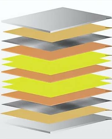
Multi-layer PCB offer significant advantages in high-density wiring, EMI suppression, short-circuit risk reduction, size compression, signal integrity, transmission rates, and thermal management for electronic applications requiring high performance and reliability.
Good PCB stacking design can provide a complete path for high-speed signal return, reduce the signal loop area, and reduce the signal coupling electrostatic discharge noise interference ability. Good PCB stack design can reduce the reference ground plane parasitic inductance, and reduce electrostatic discharge when high-frequency current flows through the ground plane generated by the ground potential difference. Good PCB stacking design, the reference ground plane, and the power plane form a good plane distribution capacitance between the system to maintain a stable power supply.
For 6 layers or more layers of the board, it must be pre-positioned for two inner layers or more inner layers of the board, so that the holes and lines of different layers have a good alignment relationship. Nail positioning: pre-drilled holes in the positioning of the inner layer of the board and the semi-cured sheet, according to the layout of the order of the set in the template equipped with nails, and then stamping nails with a nail punch to make the nails positioning. Weld positioning: pre-drilled positioning holes in the inner layer of the board and half-cured sheet, according to the layout order set in the template equipped with positioning, and then through the heating of a few fixed points, the use of half-cured sheet by the heat of the melting solidification positioning.

The main steps in manufacturing a multilayer PCB include:
- Designing the circuit layout: The circuit layout of the PCB is created using electronic design automation (EDA) software.
- Creating the Inner Layer: The inner layer is created by depositing copper foil on a thin board, then using photolithography to transfer the circuit pattern to the copper foil, and finally removing unwanted copper foil by etching.
- Stacking and pre-drilling: the inner layers are stacked together and holes are drilled between each layer for the subsequent formation of interconnecting vias.
- Adding Outer Layers: Additional layers of copper foil are added to the top and bottom of the inner layers to form the outer circuit.
- Lamination: Multiple layers of PCBs are placed into a laminating machine where heat and pressure are applied to bond the layers together.
- Drilling and Surface Finishing: Holes are drilled into the pressed PCB to create through-holes and surface finishes are applied, such as gold plating or tin spraying.
- Adding Components: Soldering electronic components into place on the PCB.
- Test and Quality Control: The finished Multilayer Lamination PCB is tested and quality controlled to ensure proper function.
Multi-layer laminated PCBs are widely used in high-density circuits and complex electronic devices such as computers, communication equipment, consumer electronics, etc. They offer smaller sizes and better performance. They have smaller dimensions, better electrical properties, and immunity to interference, and are suitable for applications requiring high performance and reliability.
The main purpose of lamination is to combine PP with different inner core boards and outer copper foils through “heat and pressure”, and to utilize the outer copper foil as the base of the outer circuit. Different PP compositions with different inner layers and copper surfaces can produce PCBs of various thicknesses. PCB pressing process is a key step in the electronic manufacturing process, in this process, the use of high temperature and high pressure to the circuit board layers bonded together, divided into kissing pressure (resin moistened bonding surface and fill the gaps in the line), full pressure (all the gaps bonded) and cold press (so that the circuit board cooled quickly and keep the size stable) process.
Common problems in the pressing process: revealing glass cloth pattern, blistering, pits, resin, wrinkles on the board surface, displacement of the inner layer of graphics, uneven thickness, inner layer slippage, misalignment between layers, board curvature, board warpage, etc. There are different solutions to the above problems, for example, for the displacement of the inner layer of graphics, analyzing the causes may be the inner layer of graphics of copper foil with low peel strength or poor temperature resistance or line width is too thin, pre-pressure is too high, the resin is too high, the dynamic viscosity is small and the press template is small. Dynamic viscosity is small and the press template is not parallel, etc., the solution is to change to a high-quality inner layer of laminate, change to a high-quality inner layer of laminate, and adjust the template.
PCB thermal pressing is a technology used to manufacture multilayer printed circuit boards (PCBs) by pressing the layers of a multilayer board together at high temperatures and under pressure. Using heat and pressure, the material is physically or chemically changed to achieve a predetermined shape and properties. The three elements of the hot press process include hot press pressure, hot press temperature, and hot press time. The hot pressing process utilizes a hot press to press the substrate, conductive layer, and insulating layer together.