I. PCB Component Layout Basic Rules
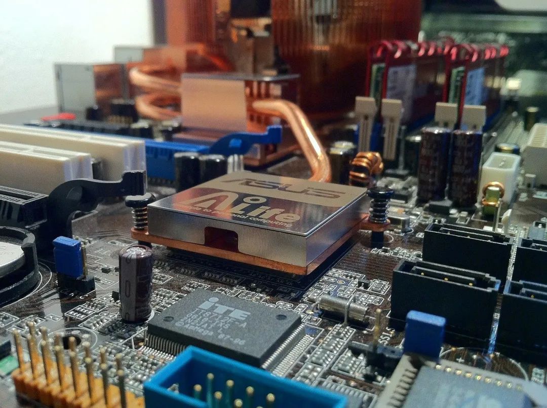
1-1. Layout by Circuit Modules: Components should be grouped according to their circuit functions (modules). Components in the same module should be placed close to each other, and digital and analog circuits should be separated.
1-2. Component Placement Near Holes: No components should be placed within I.27mm of mounting holes, positioning holes, or other non-mounting holes. For screw mounting holes, components must be placed at least III.5mm away for MII.5 screws and IVmm for MIII screws.
1-3. Avoid Placing Components Below Certain Parts: For components like horizontal resistors, power inductors (through-hole), and electrolytic capacitors, avoid placing vias directly beneath them to prevent short circuits during wave soldering.
1-4. Edge Spacing: The distance from the component’s outer edge to the board edge should be at least Vmm.
1-5. Component Spacing: The distance between the outer edges of surface-mount component pads and adjacent through-hole components should be at least IImm.
1-6. Metal Enclosure and Component Spacing: Metal-cased components (such as shielding boxes) should not touch other components or traces; the spacing should be greater than IImm. The distance between the edges of mounting holes, positioning holes, or other board holes and the board edge should be greater than IIImm.
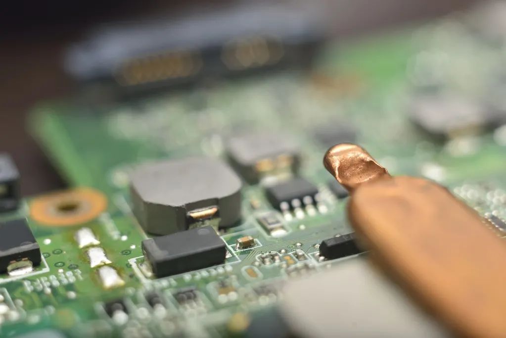
1-7. Thermal Management: Heat-producing components should not be placed too close to heat-sensitive components or traces. High-power components should be evenly distributed across the board.
1-8. Power Socket Placement: Power sockets should be placed around the edge of the PCB, with the corresponding power bus or connection terminals placed on the same side. Ensure that power connectors and other components do not interfere with each other to facilitate easy wiring and assembly.
1-9. General Component Placement: All IC components should be aligned in one direction. Polarized components should have clearly marked polarities, and there should be no more than two directions of polarity markings on a single board, with the two directions perpendicular to each other.
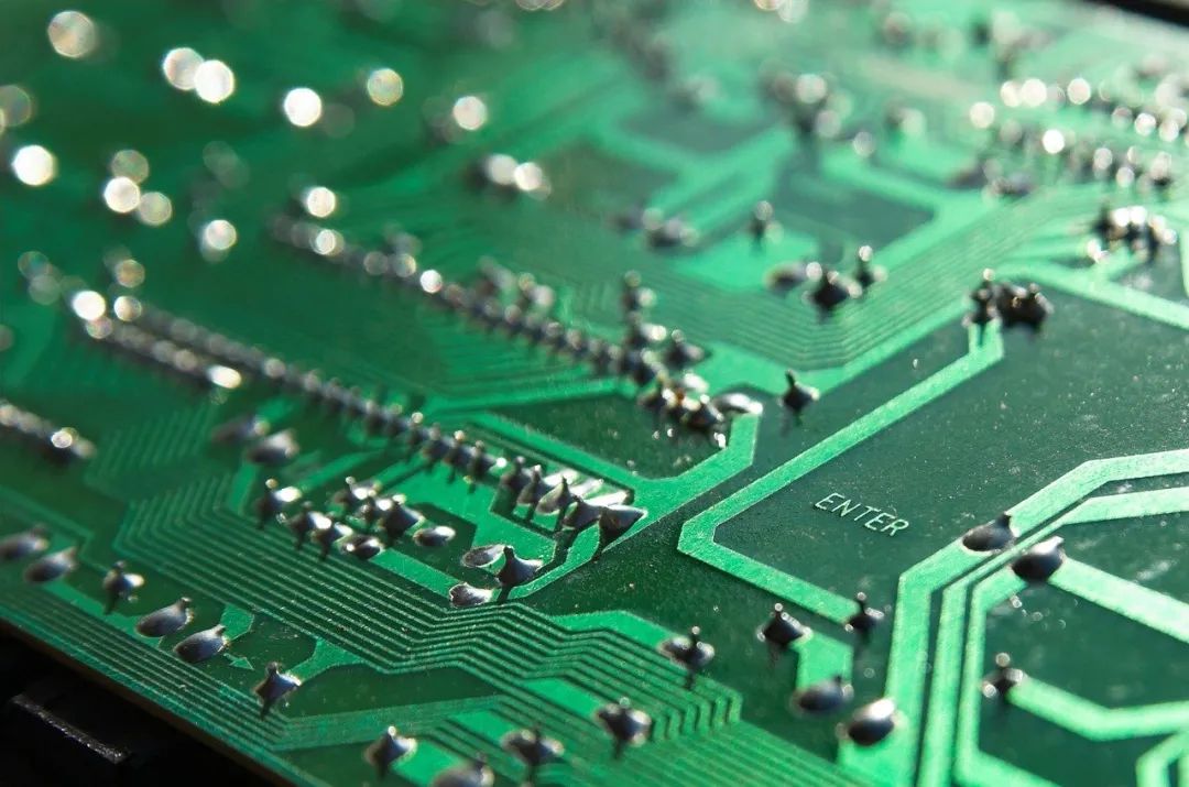
1-10. Route Density: PCB traces should be appropriately spaced. If the density varies significantly, use a mesh copper fill with a grid size of at least VIIImil (0.2mm).
1-11. Avoid Vias in SMD Pads: Vias should not be placed in surface-mount pads to avoid solder paste leakage and potential soldering issues.
1-12. Component Orientation: SMD components should be aligned on the same side of the board with consistent orientations and direction of characters.
1-13. Polarity Consistency: For polarized components, ensure the polarity markings are consistent across the PCB.
II.Improving Electromagnetic Interference (EMI) and Electromagnetic Compatibility (EMC)
1. Special Systems Requiring EMI Attention
(1) High-Frequency Microcontroller Systems: Systems with high clock frequencies and fast bus cycles.
(2) High-Power/High-Current Systems: Systems driving high-current loads or creating sparks, such as relays and large switches.
(3)Sensitive Analog Signal Systems: Systems with weak analog signals and high-precision A/D conversion circuits.

Component Layout Basic Rules
2. EMI Mitigation Measures
(1) Select Low-Frequency Microcontrollers: Choosing a microcontroller with a lower clock frequency can help reduce emitted high-frequency noise and improve system immunity to interference. Square waves tend to emit more high-frequency components than sine waves, which are less likely to generate noise.
(2) Minimize Signal Distortion: CMOS technology-based microcontrollers can cause signal reflection and distortion when connecting long traces to high-impedance inputs. Minimize trace lengths and vias, ideally keeping traces under 25cm and limiting the number of vias to two or fewer.
(3) Reduce Crosstalk Between Signal Lines: Signal interference occurs when signals transmitted along one trace interfere with those in adjacent traces. To reduce this, use large ground planes under sensitive signal traces and ensure proper trace spacing (at least 2-3 times the trace width).
(4) Minimize Power Supply Noise: Power supply lines often introduce noise into the system. Use proper decoupling capacitors (e.g., 0.1µF and 1µF ceramic capacitors) to filter high-frequency noise and stabilize power delivery. Always decouple power and ground connections for each IC.
(5) High-Frequency Characteristics of PCB layout: For high-speed designs, consider the parasitic inductance and capacitance of traces, vias, and components. Avoid trace lengths that are a significant fraction of the wavelength of the noise frequency to prevent them from acting as antennas. For example, vias add around 0.6pF of capacitance.
(6) Component Layout for EMI: Properly separate noisy components (e.g., relays, high-current switches) from sensitive analog circuitry to minimize cross-coupling. Keep digital and analog grounds separate and ensure they meet at a single point (single-point grounding).
(7) Use Shielding for Sensitive Circuits: High-frequency or noise-sensitive circuits should be shielded using metal enclosures or PCB-level shielding techniques.
(8) Use Effective Decoupling Capacitors: Capacitors with good high-frequency performance, such as multilayer ceramic capacitors, can effectively filter high-frequency noise. Place decoupling capacitors close to IC power pins and ensure they provide adequate filtering for both the IC’s power and ground pins.
(9) Minimize Through-Hole Use: Through-holes can introduce unwanted inductance, especially in high-speed circuits. Use them sparingly and avoid routing high-frequency signals through vias.

III. Some experience in reducing noise and electromagnetic interference.
(1) If low-speed chips can be used, high-speed chips should not be used. High-speed chips should be used in key places.
(2) A resistor can be used in series to reduce the jump rate of the upper and lower edges of the control circuit.
(3) Try to provide some form of damping for relays, etc.
(4) Use a low-frequency clock that meets the system requirements.
(5) The clock generator should be as close as possible to the device using the clock. The quartz crystal oscillator housing should be grounded.
(6) Use a ground wire to circle the clock area and keep the clock line as short as possible.
(7) The I/O drive circuit should be as close as possible to the edge of the PCB to make it leave the printed circuit board as soon as possible. The signal entering the PCB should be filtered, and the signal coming from the high noise area should also be filtered. At the same time, the terminal resistor should be used in series to reduce signal reflection.
(8) The unused end of the MCD should be connected to a high, or grounded, or defined as an output end. The ends of the integrated circuit that should be connected to the power ground should be connected and not left floating.
(9) Do not leave unused gate inputs floating. The unused op amp positive input should be grounded and the negative input connected to the output.
(10) Try to use 45° zigzag lines instead of 90° zigzag lines for printed circuit boards to reduce the emission and coupling of high-frequency signals.
(11) Printed circuit boards are divided according to frequency and current switching characteristics. Noise components and non-noise components should be farther apart.
(12) Single-sided and double-sided boards should use single-point power supply and single-point grounding. The power line and ground line should be as thick as possible. If the economy can afford it, use multi-layer boards to reduce the capacitance and inductance of the power supply and ground.
(13) Clock, bus, and chip select signals should be kept away from I/O lines and connectors.
(14) Analog voltage input lines and reference voltage terminals should be kept away from digital circuit signal lines, especially clocks.
(15) For A/D devices, it is better to unify the digital and analog parts rather than cross them. (16) Clock lines perpendicular to I/O lines have less interference than parallel I/O lines. Clock component pins should be kept away from I/O cables.
(17) Component pins should be as short as possible, and decoupling capacitor pins should be as short as possible.

(18) Key lines should be as thick as possible, and protective ground should be added on both sides. High-speed lines should be short and straight.
(19) Noise-sensitive lines should not be parallel to high-current, high-speed switching lines.
(20) Do not run lines under quartz crystals or under noise-sensitive devices.
(21) Do not form current loops around weak signal circuits and low-frequency circuits.
(22) Do not form loops for any signal. If unavoidable, keep the loop area as small as possible.
(23) One decoupling capacitor for each integrated circuit. A small high-frequency bypass capacitor should be added next to each electrolytic capacitor.
(24) Use large-capacity tantalum capacitors or polycool capacitors instead of electrolytic capacitors as circuit charging and discharging energy storage capacitors. When using tubular capacitors, the casing should be grounded.
iPCB mainly shares how to reduce noise and electromagnetic interference in analog circuit design through reasonable PCB layout and routing rules, grounding, decoupling capacitors, filtering and shielding, thereby improving the circuit's anti-interference ability and signal stability.